Photosensitive device and preparation method thereof, display substrate and method for detecting light intensity

A technology for photosensitive devices and display substrates, which can be used in electric solid-state devices, semiconductor devices, electrical components, etc., and can solve problems such as poor light intensity accuracy

Active Publication Date: 2019-05-17
BOE TECH GRP CO LTD
View PDF4 Cites 5 Cited by
  • Summary
  • Abstract
  • Description
  • Claims
  • Application Information

AI Technical Summary

Problems solved by technology

[0005] The present invention at least partly solves the problem of poor accuracy of light intensity detected by existing photosensitive dev

Method used


Image

  • Photosensitive device and preparation method thereof, display substrate and method for detecting light intensity
  • Photosensitive device and preparation method thereof, display substrate and method for detecting light intensity
  • Photosensitive device and preparation method thereof, display substrate and method for detecting light intensity

Examples


Embodiment 1

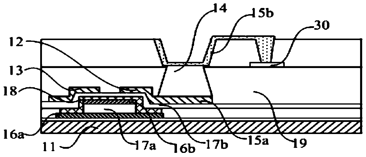
[0040] Such as figure 2 As shown in Figure 3, this embodiment provides a photosensitive device, including:

[0041] Substrate 11;

[0042] A double-gate transistor located on the substrate 11, the double-gate transistor includes a first gate 12 and a second gate 13;

[0043] A photosensitive structure for photosensitization, which includes:

[0044] The photosensitive structure layer 14 can receive external light and generate corresponding charges according to different light intensity;

[0045] The first pole 15a and the second pole 15b are respectively connected to the photosensitive structure layer 14 , and the first pole 15a is connected to the first grid 12 .

[0046] Among them, the first gate 12 in the double-gate transistor is used to connect with the photosensitive structure, and the photosensitive structure can transmit the voltage generated by the charge after illumination to the double-gate transistor through the first gate 12, that is, the voltage of the first...

Embodiment 2

[0075] Such as figure 2 As shown in FIG. 3, the present embodiment provides a method for preparing a photosensitive device, the photosensitive device is the photosensitive device in Example 1, and the method includes:

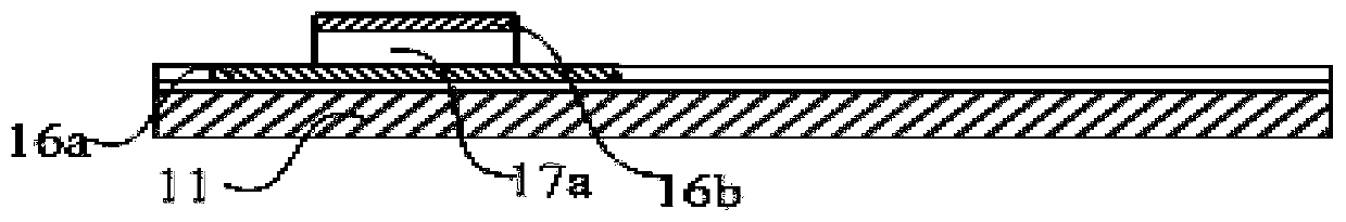
[0076] A double-gate transistor and a photosensitive structure are formed on the substrate 11 .

[0077] Specifically, forming a double-gate transistor includes: sequentially forming a first electrode 16a, a first dielectric layer 17a, a second electrode 16b, an active layer 18, a second dielectric layer 17b, and the first gate 12 on the substrate 11. and the second grid 13 .

[0078] The specific steps of forming a double-gate transistor and a photosensitive structure on the substrate 11 are as follows:

[0079] S201, such as Figure 3a As shown, a first electrode 16a is formed on the substrate 11, and the first electrode 16a has two spaced connection regions and a non-connection region between the two connection regions.

[0080] S202, such as Figure 3...

Embodiment 3

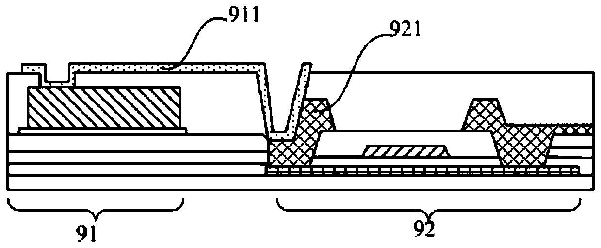
[0090] Such as figure 2 As shown in FIG. 3, this embodiment provides a display substrate, including:

[0091] The photosensitive device in embodiment 1;

[0092] A display device, the display device includes a driving transistor 21 and a light emitting structure 22 connected to the drain of the driving transistor 21 . The light emitting structure 22 includes a cathode, an anode and a light emitting layer.

[0093] Among them, the display of the display device can be adjusted according to the external light intensity detected by the photosensitive device, for example, the automatic dimming of the display substrate can be realized; or, the touch control of the display substrate and the recognition of fingerprints can also be realized according to the detection results of the photosensitive device. .

[0094] Preferably, the display substrate of this embodiment further includes: a pixel defining layer 23 for defining a light-emitting area; the light-emitting structure 22 is a...


PUM


Abstract

The invention provides a photosensitive device and a preparation method thereof, a display substrate and a method for detecting light intensity, belongs to the technical field of display, and can at least partially solve the problem of poor accuracy of light intensity detected by the existing photosensitive device. A photosensitive device provided by the invention comprises a substrate; a dual-gate transistor located on the substrate and comprising a first gate and a second gate; a photosensitive structure for sensitization comprising a photosensitive structure layer capable of receiving external light and generating corresponding electric charges according to different light intensities; and a first pole and a second pole respectively connected to the photosensitive structure layer, wherein the first pole is connected to the first gate.

Description

technical field [0001] The invention belongs to the field of display technology, and in particular relates to a photosensitive device, a preparation method thereof, a display substrate, and a light intensity detection method. Background technique [0002] In recent years, with the rapid development of science and technology, products with photosensitive devices have gradually entered people's lives and work, such as touch mobile terminals, fingerprint recognition, pulse detection, etc. [0003] Such as figure 1 As shown, a photosensitive device in the prior art mainly includes a photosensitive structure 91 and a transistor 92 , and an electrode 911 of the photosensitive structure 91 is connected to a source 921 of the transistor 92 . Wherein, the photosensitive structure 91 can receive external light and generate different currents according to different light intensity, and output through the transistor 92 to control the light emitting device or other devices. [0004] Ho...

Claims


Application Information

Patent Timeline
IPC IPC(8): H01L27/144H01L27/32G01J1/42
Inventor 彭锦涛高雪岭彭宽军张方振史鲁斌牛亚男秦纬
Owner BOE TECH GRP CO LTD
Why Eureka
Try Eureka