Chip apparent defect detection method

A defect detection and appearance technology, applied in measuring devices, image data processing, instruments, etc., can solve problems such as false detection, high work intensity, and limitation of SOP chip accuracy

Active Publication Date: 2019-05-21
HUNAN UNIV
View PDF3 Cites 22 Cited by
  • Summary
  • Abstract
  • Description
  • Claims
  • Application Information

AI Technical Summary

Problems solved by technology

[0002] In the production process of chip devices, the apparent quality inspection of the chip is one of the essential links. At present, the apparent quality inspection of the SOP chip of the integrated circuit mainly adopts the artificial eye inspection method, which has high work intensity and is easy to cause false detection, and The detection speed and accuracy are low, which makes the detection efficiency low and cannot meet the requirements of large-scale production of enterprises. The above factors have restricted the development of my country's integrated chip production industry to a large extent.
[0003] At present, some inherent defects also limit the accuracy of SOP chip detection to a certain extent, such as detection speed and accuracy

Method used


Image

  • Chip apparent defect detection method
  • Chip apparent defect detection method
  • Chip apparent defect detection method

Examples


Embodiment Construction

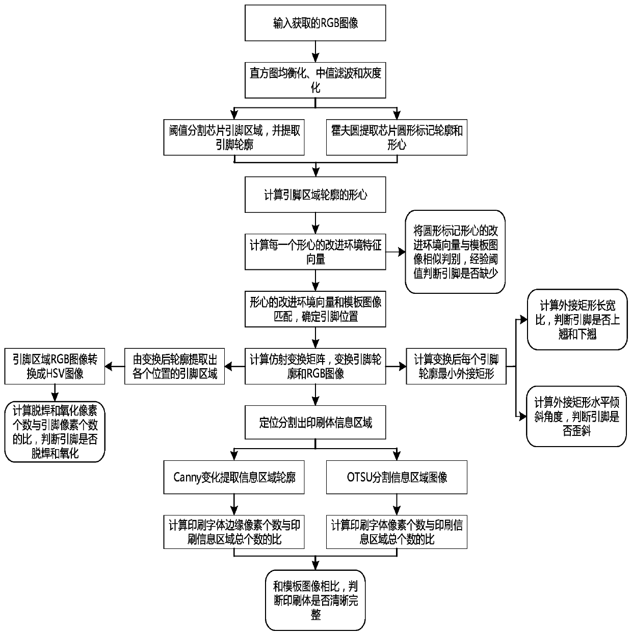
[0097] The present invention will be further described below with reference to the accompanying drawings and examples, and the embodiments of the present invention include but not limited to the following examples.

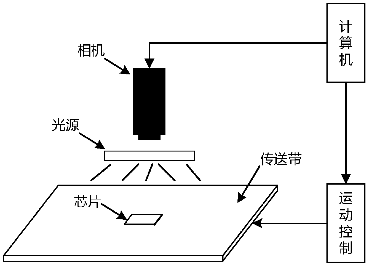
[0098] figure 2 It is a schematic diagram of the hardware structure of the SOP chip defect detection system of the present invention. Before detection, an industrial color CCD camera and light source should be installed above the target chip. The computer controls the camera to shoot and the conveyor belt to move. When the chip moves to the bottom of the camera, the chip is photographed. During the detection, it is required that there is no object interference around the chip, the background of the conveyor belt is black, and at the same time, the light is sufficient, the circular mark is clearly illuminated, the pin brightness is relatively high, and the camera resolution is clear enough.

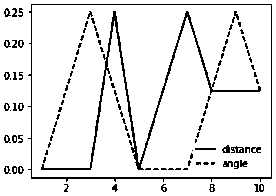
[0099] image 3 A modified environment vector representing a circular ...


PUM


Abstract

The invention discloses a chip apparent defect detection method. The method comprises: an SOP chip image is shot by using a color CCD camera; extracting the circular mark of the chip and the contour and the centroid of the pin through a series of pretreatment; calculating improved environment feature vectors of the circular mark and each centroid of the pin; matching and positioning with a template image are carried out; calculating an affine transformation matrix; carrying out affine transformation on the image to obtain a template image coordinate system; and finally, judging whether the pins are lacked or not according to the improved environment vector of the circular mark. printing pixels are extracted from the printing area, the edge of the printing area is used for judging whether printing information is defective or not, a minimum circumscribed rectangle is calculated for the outline of each pin to judge whether the pins are warped upwards, warped downwards and skewed or not, and oxidation and desoldering pixels are extracted from the pin area to judge whether the pins are oxidized or desoldered or not. The method can automatically, quickly, conveniently and accurately judge the problems of lack, upwarp, downwarp, skew, desoldering and oxidation of the SOP chip pins, can also judge whether a printing information area is clear and complete or not, can effectively detectthe appearance of an SOP chip product, and reduces the labor intensity of workers.

Description

technical field [0001] The invention relates to a chip apparent defect detection method, which belongs to the field of machine vision detection, and is an integrated circuit packaging (SOP) chip apparent defect detection method based on an improved environment vector rapid positioning technology. Background technique [0002] In the production process of chip devices, the apparent quality inspection of the chip is one of the essential links. At present, the apparent quality inspection of the SOP chip of the integrated circuit mainly adopts the artificial eye inspection method, which has high work intensity and is easy to cause false detection, and The detection speed and accuracy are low, which makes the detection efficiency low and cannot meet the requirements of large-scale production of enterprises. The above factors have restricted the development of my country's integrated chip production industry to a large extent. [0003] At present, some inherent defects also limit t...

Claims


Application Information

Patent Timeline
Patent Type & Authority Applications(China)
IPC IPC(8): G06T7/00G06T7/11G06T7/136G06T7/30G01N21/956
Inventor 袁小芳刘琛田争鸣王浩然陈祎婧肖祥慧
Owner HUNAN UNIV
Why Eureka
Try Eureka