Supercharge Your Innovation With Domain-Expert AI Agents!

Method for forming fin field effect transistor (finfet) device structure

A technology of field effect transistor and device structure, applied in the field of fin field effect transistor device structure and its manufacture

Inactive Publication Date: 2019-05-21
TAIWAN SEMICON MFG CO LTD
View PDF0 Cites 0 Cited by
  • Summary
  • Abstract
  • Description
  • Claims
  • Application Information

AI Technical Summary

Problems solved by technology

[0004] While existing FinFET devices and methods of fabricating FinFET devices are generally adequate for their intended purposes, they have not been completely satisfactory in all respects

Method used


Image

  • Method for forming fin field effect transistor (finfet) device structure
  • Method for forming fin field effect transistor (finfet) device structure
  • Method for forming fin field effect transistor (finfet) device structure

Examples


Embodiment Construction

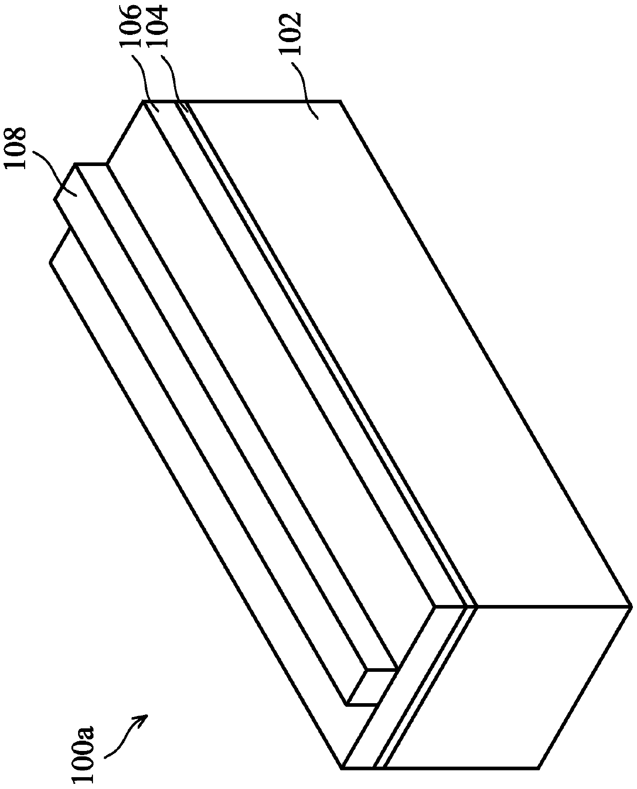
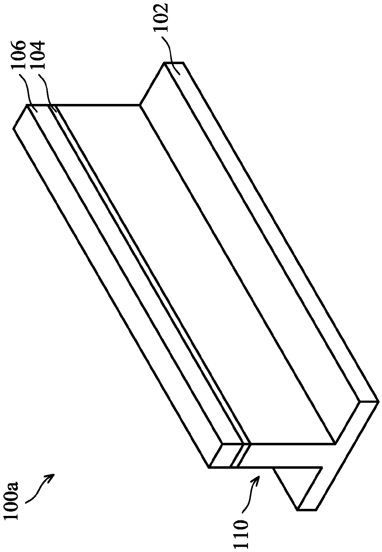
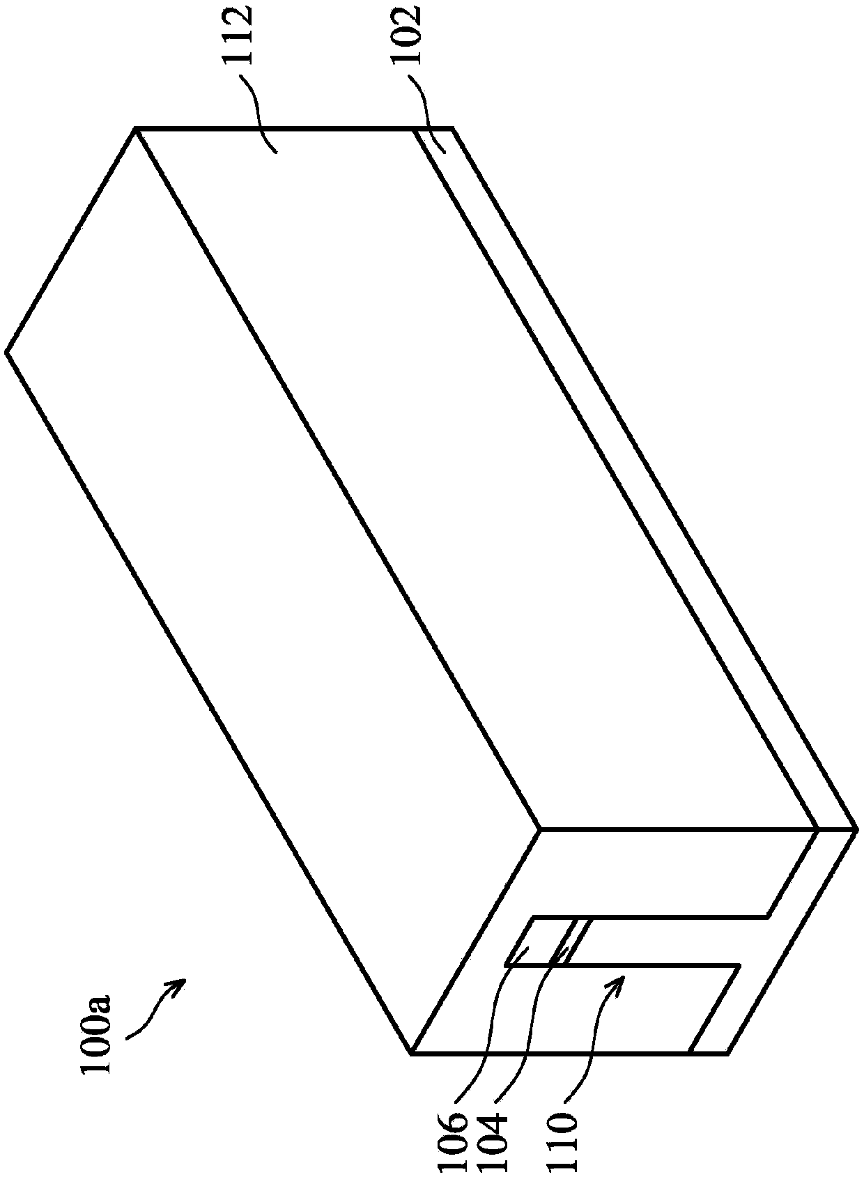
[0061] The following presents a number of different embodiments, or examples, for implementing different components of the presented subject matter. Specific examples of components and configurations are described below to simplify embodiments of the invention. Of course, these are just examples, not intended to limit the embodiments of the present invention. For example, if the description mentions that a first part is formed above a second part, it may include an embodiment where the first and second parts are in direct contact, and may also include an additional part formed between the first and second parts , such that the first and second components are not in direct contact. In addition, the embodiments of the present invention may repeat reference numerals and / or letters in different examples. This repetition is for the purpose of simplification and clarity, and does not mean that there is a specific relationship between the different embodiments and / or configurations ...


PUM


Abstract

A method for forming a FinFET device structure is provided. The method includes forming a gate structure over a fin structure. The method also includes forming an S / D contact structure over a S / D structure and depositing a protection layer over the S / D contact structure. The portion layer and the S / D contact structure are made of different materials. The method further includes forming an etchingstop layer over the protection layer and forming a dielectric layer over the etching stop layer. The method includes forming a first recess through the dielectric layer and the etching stop layer to expose the protection layer and forming an S / D conductive plug in the first recess. The S / D conductive plug includes a barrier layer directly on the protection layer, and the protection layer and the barrier layer are made of different materials.

Description

technical field [0001] Embodiments of the present invention relate to semiconductor manufacturing technology, and in particular to the structure of a fin field effect transistor device and its manufacturing method. Background technique [0002] Semiconductor devices are used in various electronic applications such as personal computers, mobile phones, digital cameras, and other electronic equipment. Usually by sequentially depositing insulating or dielectric layer, conductive layer and semiconductor layer material on the semiconductor substrate, and using lithography (lithography) to pattern the various material layers to form circuit components and components on the semiconductor substrate. A semiconductor device is manufactured. Many integrated circuits are typically fabricated on a single semiconductor wafer, and individual dies on the wafer are singulated by sawing along scribe lines between the integrated circuits. Individual chips are typically packaged separately, s...

Claims


Application Information

Patent Timeline
IPC IPC(8): H01L21/331H01L29/739H01L29/06
CPCH01L29/41791H01L29/66795H01L29/785H01L21/76897H01L21/76883H01L21/76849H01L21/28562H01L21/76831H01L23/485H01L23/53209H01L23/5226H01L21/7684H01L21/76844
Inventor 陈健源李振铭杨复凯王美匀
Owner TAIWAN SEMICON MFG CO LTD
Features
  • R&D
  • Intellectual Property
  • Life Sciences
  • Materials
  • Tech Scout
  • Unparalleled Data Quality
  • Higher Quality Content
  • 60% Fewer Hallucinations
Learn More