Preparation method for organic light emitting diode display device and display device

A technology for light-emitting diodes and display devices, which is applied in the fields of organic semiconductor devices, photovoltaic power generation, semiconductor/solid-state device manufacturing, etc., can solve problems such as device failure, and achieve the effect of improving water and oxygen resistance and ensuring packaging reliability

Inactive Publication Date: 2019-05-21
BOE TECH GRP CO LTD
View PDF6 Cites 30 Cited by
  • Summary
  • Abstract
  • Description
  • Claims
  • Application Information

AI Technical Summary

Problems solved by technology

However, in the prior art, when the screen is opened, the evaporated film layer cannot be cut off in the display area, and the side of the display area will be exposed to the atmosphere and invaded by water and oxygen, which will cause the device to fail quickly.

Method used


Image

  • Preparation method for organic light emitting diode display device and display device
  • Preparation method for organic light emitting diode display device and display device
  • Preparation method for organic light emitting diode display device and display device

Examples


preparation example Construction

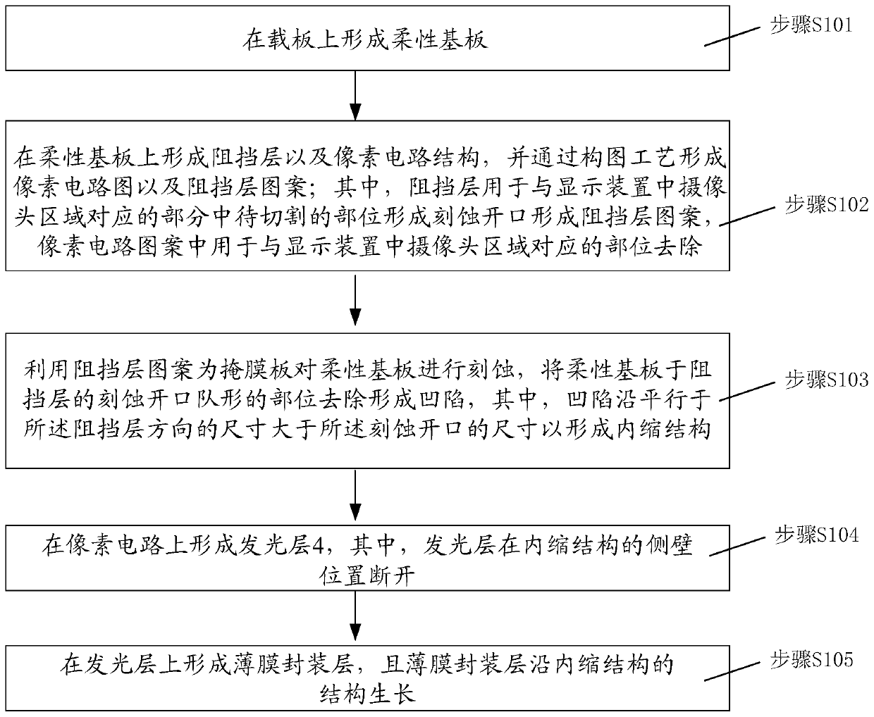
[0036] Please refer to figure 1 , the invention provides a method for preparing an organic light emitting diode display device, comprising:

[0037] Step S101: forming a flexible substrate 1 on a carrier;

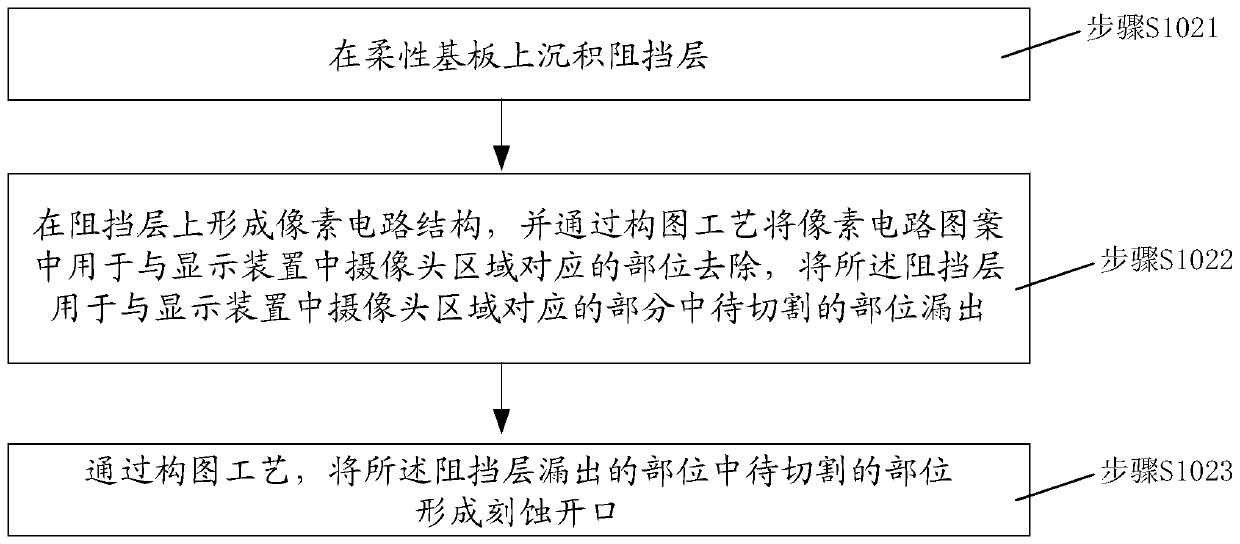
[0038] Step S102: Form a barrier layer 2 and a pixel circuit structure 3 on the flexible substrate 1, and form a pixel circuit through a patterning process image 3 And the barrier layer 2 pattern; wherein, the barrier layer 2 is used to form an etching opening in the part to be cut in the part corresponding to the camera area in the display device to form a barrier layer pattern, and the pixel circuit pattern is used in the pixel circuit pattern corresponding to the camera area in the display device site removal;

[0039] Step S103: Etching the flexible substrate 1 by using the barrier layer pattern as a mask, removing the flexible substrate at the position of the etching opening formation of the barrier layer to form a depression, wherein the depression is along a dimen...

Embodiment example

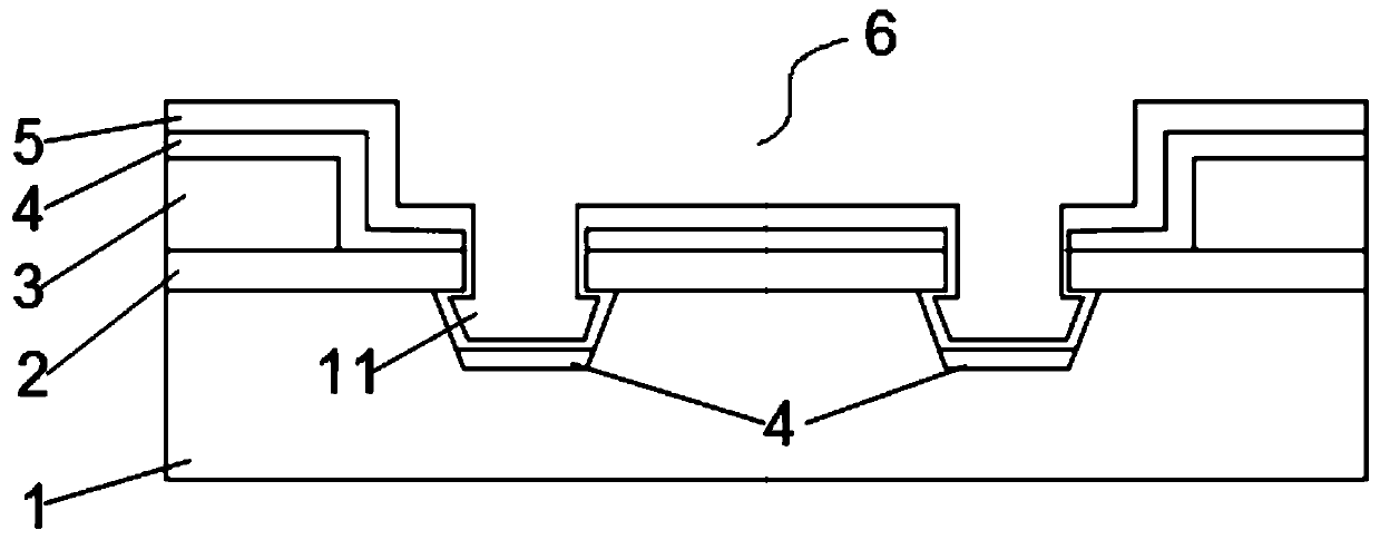
[0055] As a possible implementation example of the above-mentioned thin film encapsulation layer, the thin film encapsulation layer 5 includes a first organic layer, an inorganic layer, and a second organic layer located on the side of the inorganic layer away from the first organic layer, wherein the first organic layer is The sidewall position of the retracted structure is disconnected. Since the organic layer has a greater effect on the thin film encapsulation layer 5 to improve flatness and reduce mechanical damage, and at the same time, because the light-emitting layer 4 is disconnected at the inner shrinkage structure 11, the first organic layer is omitted, and materials are also saved. .

[0056] In addition, the present invention also provides a display device, such as image 3 As shown, it includes: a flexible substrate 1, a barrier layer 2, a pixel circuit structure 3, a light emitting layer 4 and a thin film encapsulation layer 5, wherein the side of the flexible s...


PUM


Abstract

The invention provides a preparation method for organic light emitting diode display device and the display device. The preparation method comprises the steps of forming a flexible substrate on a support plate; forming a blocking layer and a pixel circuit structure on the flexible substrate, and forming a pixel circuit diagram and a blocking layer pattern through utilization of a composition technology; etching the flexible substrate through utilization of the blocking layer pattern as a mask plate, and removing parts of the flexible substrate corresponding to etching openings of the blockinglayer to form sunken parts, wherein sizes of the sunken parts along a direction of the blocking layer are greater than those of the etching openings, thereby forming inward retraction structures; forming a light emitting layer on a pixel circuit, wherein the light emitting layer is disconnected at positions of side walls of the inward retraction structures; and forming a thin film packaging layeron the light emitting layer, wherein the thin film packaging layer grows along the structures of the inward retraction structures. According to the preparation method provided by the invention, aftera hole is set on the display device, a packaging effect of a hole area can be ensured, packaging reliability of the device is ensured.

Description

technical field [0001] The invention relates to the field of flexible organic light emitting diode display devices, in particular to a method for preparing an organic light emitting diode display device and a display device. Background technique [0002] Organic light emitting diode display devices are increasingly being used in electronic products, especially after the concept of a full screen was proposed, they have been in the process of continuous improvement and realization. For a full screen, the camera area is an area that is very difficult to bypass in the process of realizing a full screen, because the camera area needs to open a hole in the display area. However, in the prior art, when the screen is opened, the evaporated film layer cannot be cut off in the display area, and the side of the opening in the display area will be exposed to the atmosphere and invaded by water and oxygen, so that the device will fail quickly. Contents of the invention [0003] The in...

Claims


Application Information

Patent Timeline
Patent Type & Authority Applications(China)
IPC IPC(8): H01L27/32H01L51/50H01L51/52H01L51/56
CPCY02E10/549H10K59/122H10K71/231H10K77/111H10K59/1201H10K50/844H10K71/00H10K71/164H10K71/233H10K2102/311H10K2102/351
Inventor 谢春燕张嵩王品凡王涛谷朋浩
Owner BOE TECH GRP CO LTD
Why Eureka
Try Eureka