Manufacturing method of golden finger circuit board

A production method and gold finger technology, applied in the direction of printed circuit manufacturing, printed circuits, electrical components, etc., to achieve the effect of optimizing the production process and enhancing the ability of sealing grooves

Active Publication Date: 2019-05-21
JIANGMEN SUNTAK CIRCUIT TECH
View PDF13 Cites 15 Cited by
  • Summary
  • Abstract
  • Description
  • Claims
  • Application Information

AI Technical Summary

Problems solved by technology

[0006] The present invention aims at the above-mentioned problems in the prior art of making a gold-finger circuit board with gold-plated gold on three sides, and provides a method for making a gold-finger circuit board that can realize three-side gold-plated gold-finger and nickel-gold-impregnated PAD on the board surface. It is suitable for the production of gold finger circuit boards with a board thickness less than 1.0mm and a gold finger side wall groove larger than 2.5mm×9mm. The gold surface of the gold finger has no quality problems such as copper plating, pollution, and double nickel gold

Method used


Image

  • Manufacturing method of golden finger circuit board
  • Manufacturing method of golden finger circuit board
  • Manufacturing method of golden finger circuit board

Examples


Embodiment

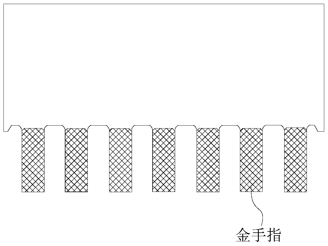
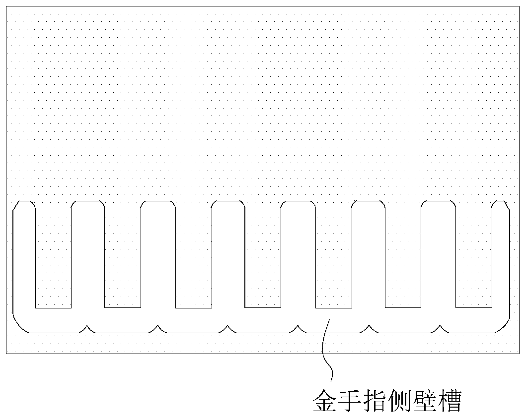
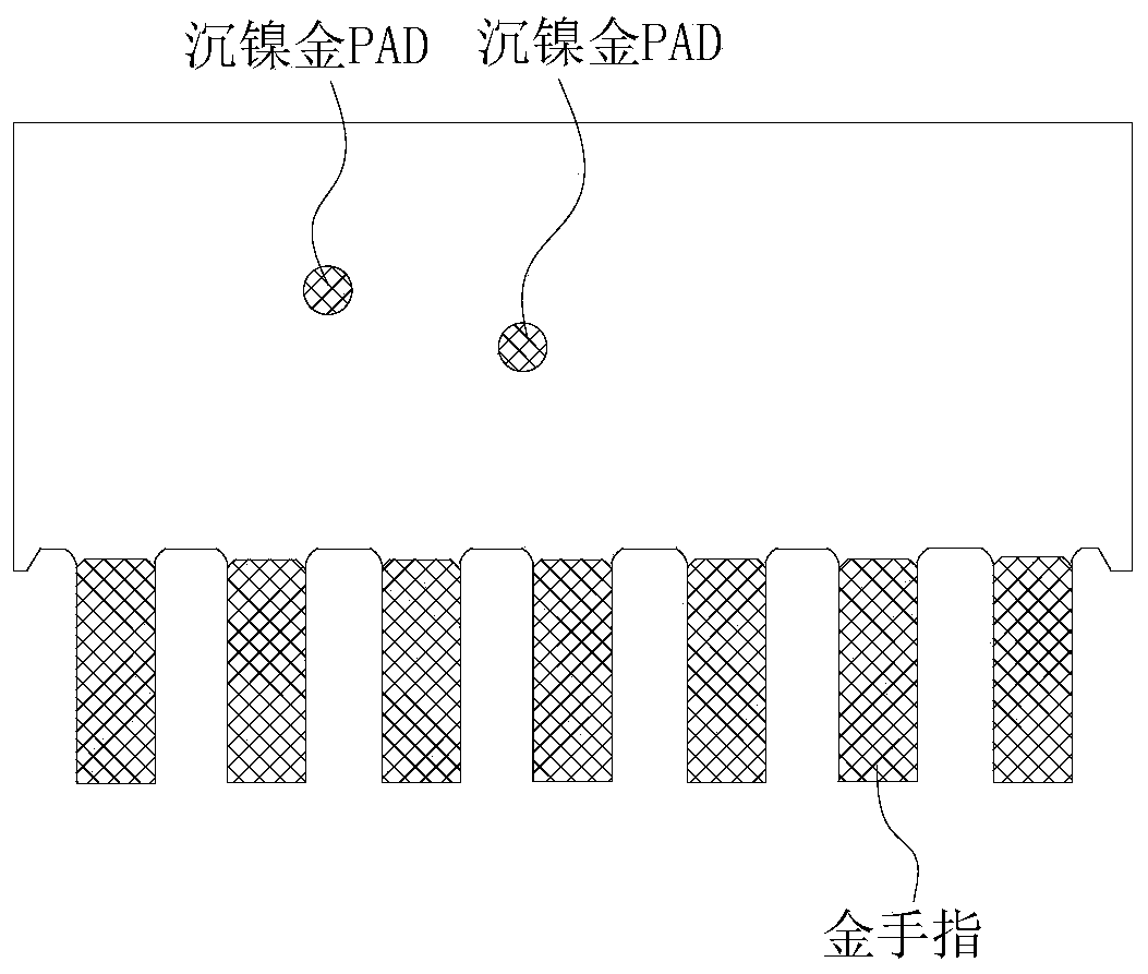
[0030] This embodiment provides a method for manufacturing a gold finger circuit board. The thickness of the produced gold finger circuit board is less than 1mm, the three sides of the gold finger are plated with gold, the side wall groove of the gold finger is larger than 2.5mm×9mm, and the PAD on the board surface is sunk Nickel gold finish.

[0031] The board surface of the production board processed in the production process is divided into a circuit area and a gold finger area, and the gold finger area includes a gold finger position for making a gold finger and a side wall groove for making a gold finger side wall groove, and the manufacturing method as follows:

[0032] (1) Cutting: cut out the inner core board according to the panel size required by the design.

[0033] (2) Fabricate the inner layer circuit: adopt the negative process to fabricate the inner layer circuit on the inner layer core board to obtain the inner layer circuit board. After etching the inner la...


PUM


Abstract

The invention relates to the technical field of printed circuit boards, and in particular to a manufacturing method of a golden finger circuit board. According to the manufacturing method provided bythe invention, an adhesive tape is laminated in a golden finger area at first before an outer layer circuit pattern is electroplated to improve the groove sealing ability of a dry film, so as to prevent liquid medicine from infiltrating during electrocoppering and electrotinning to plate copper and tin on the golden finger; a golden finger area pattern is not only manufactured before tin removal to cover the golden finger area, the adhesive tape is also laminated in the golden finger area to improve the groove sealing ability of a dry film, so as to prevent the tin removal liquid medicine frominfiltrating to etch a golden surface of the golden finger; and before nickel and gold are deposited on PAD, the adhesive tape is laminated in the golden finger area to seal a groove on the side wallof the golden finger, so as to prevent nickel and gold deposition liquid medicine from infiltrating to form double-layer nickel and gold on the golden finger, therefore the manufacture of the circuitboard having the golden finger with three gilded surfaces and the PAD with the deposited nickel and gold is achieved.

Description

technical field [0001] The invention relates to the technical field of printed circuit boards, in particular to a method for manufacturing a golden finger circuit board. Background technique [0002] In the field of printed circuit boards, gold fingers are often designed on circuit boards such as memory sticks, graphics cards, network cards, etc., which are equipped with electronic components, as a connecting part between such circuit boards and slots. Gold fingers are composed of many golden yellow conductive contacts arranged in the same order. Because the surface is gold-plated and the conductive contacts are arranged in a finger shape, they are called "gold fingers". This kind of circuit with gold fingers is designed on the edge or inside the board The board is called a gold finger circuit board. [0003] The conventional manufacturing process of the gold finger circuit board includes designing a lead wire connected to the edge of the metal plate at the outer end of the...

Claims


Application Information

Patent Timeline
Patent Type & Authority Applications(China)
IPC IPC(8): H05K3/40H05K3/00
Inventor 寻瑞平黄少南戴勇刘红刚李显流
Owner JIANGMEN SUNTAK CIRCUIT TECH
Why Eureka
Try Eureka