Supercharge Your Innovation With Domain-Expert AI Agents!

Array substrate and its preparation method and display screen

A technology for array substrates and display screens, applied in identification devices, instruments, organic semiconductor devices, etc., can solve problems such as easy breakage of metal wiring, and achieve the effects of improving screen yield, avoiding breakage, and reducing pressure

Active Publication Date: 2021-04-20
KUNSHAN GO VISIONOX OPTO ELECTRONICS CO LTD
View PDF14 Cites 0 Cited by
  • Summary
  • Abstract
  • Description
  • Claims
  • Application Information

AI Technical Summary

Problems solved by technology

[0004] Based on this, it is necessary to provide an array substrate that is not easy to cause metal wires to break due to the problem that metal wires are easy to break in the prior art

Method used


Image

  • Array substrate and its preparation method and display screen
  • Array substrate and its preparation method and display screen

Examples


Embodiment Construction

[0033] In order to make the object, technical solution and advantages of the present invention clearer, the present invention will be further described in detail below in conjunction with specific embodiments. It should be understood that the specific embodiments described here are only used to explain the present invention, and are not intended to limit the present invention.

[0034] Unless otherwise defined, all technical and scientific terms used herein have the same meaning as commonly understood by one of ordinary skill in the technical field of the invention. The terminology used herein in the description of the present invention is only for the purpose of describing specific embodiments, and is not intended to limit the present invention. As used herein, the term "and / or" includes any and all combinations of one or more of the associated listed items.

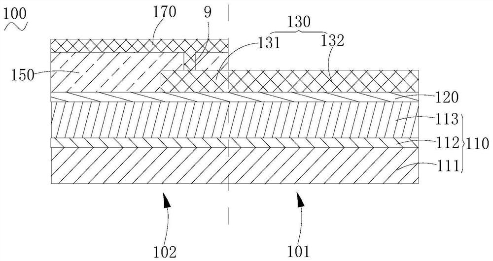
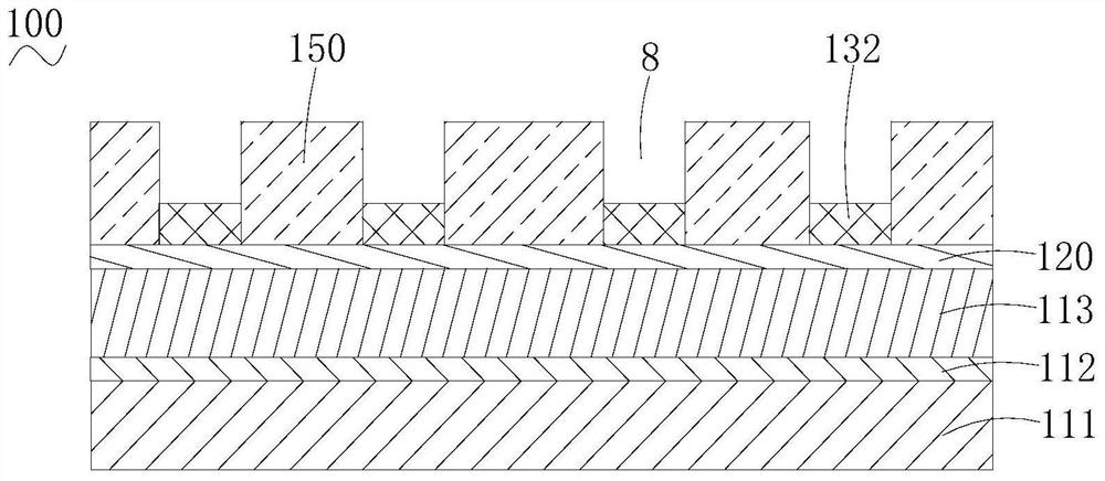
[0035] An array substrate according to an embodiment of the present invention has a display area and a non-display a...


PUM

PropertyMeasurementUnit
thicknessaaaaaaaaaa
thicknessaaaaaaaaaa

Abstract

The invention relates to an array substrate, comprising a substrate; an external wiring formed on the substrate; the external wiring includes an external section and a line change section located inside the external section; an inorganic film layer covers the external wiring On the line; the inorganic film layer is provided with a via hole for partially leaking the line change section, and a groove for leaking the outer connection section; and a metal layer, formed on the inorganic film layer; the metal layer includes a plurality of metal wires; The metal trace is electrically connected to the wire-changing segment through the via hole. In the above-mentioned array substrate, there is no inorganic film layer above the outer section, so that the inorganic film layer is prevented from being squeezed on the outer section during bending, the stress is reduced, and the outer section is prevented from breaking. The invention also provides a preparation method of the array substrate and a display screen.

Description

technical field [0001] The invention relates to the field of display technology, in particular to an array substrate, a preparation method thereof, and a display screen. Background technique [0002] The display screen includes a display area (AA area) and a non-display area (non-AA area). In order to achieve certain functions, the non-display area is required to be bendable. For example, in order to achieve a narrow frame, the non-display area is bent to the back of the screen, thereby reducing the width of the frame. [0003] However, in the current display screen, during the bending process of the non-display area, the film layer in the non-display area breaks, which in turn causes the metal wires to break easily, resulting in a defective screen body. Contents of the invention [0004] Based on this, it is necessary to provide an array substrate that is less likely to cause breakage of the metal wires to solve the problem that the metal wires are easily broken in the p...

Claims


Application Information

Patent Timeline
Patent Type & Authority Patents(China)
IPC IPC(8): G09F9/30
CPCH01L33/08H01L33/44H01L33/62G09F9/30H01L27/1244H10K59/131H10K71/00H10K2102/311H10K71/231H01L27/124H10K19/20
Inventor 李瑶
Owner KUNSHAN GO VISIONOX OPTO ELECTRONICS CO LTD
Features
  • R&D
  • Intellectual Property
  • Life Sciences
  • Materials
  • Tech Scout
  • Unparalleled Data Quality
  • Higher Quality Content
  • 60% Fewer Hallucinations
Learn More