Preparation method of light emitting display

A technology for a light-emitting display and a manufacturing method, which is applied in the direction of electric solid-state devices, semiconductor devices, electrical components, etc., and can solve problems such as low efficiency

Active Publication Date: 2019-06-14
INTERFACE TECH CHENGDU CO LTD +2
View PDF3 Cites 8 Cited by
  • Summary
  • Abstract
  • Description
  • Claims
  • Application Information

AI Technical Summary

Problems solved by technology

However, for displays containing millions of pixels, such a process can take hours to complete and is therefore inefficient

Method used


Image

  • Preparation method of light emitting display
  • Preparation method of light emitting display
  • Preparation method of light emitting display

Examples


Embodiment Construction

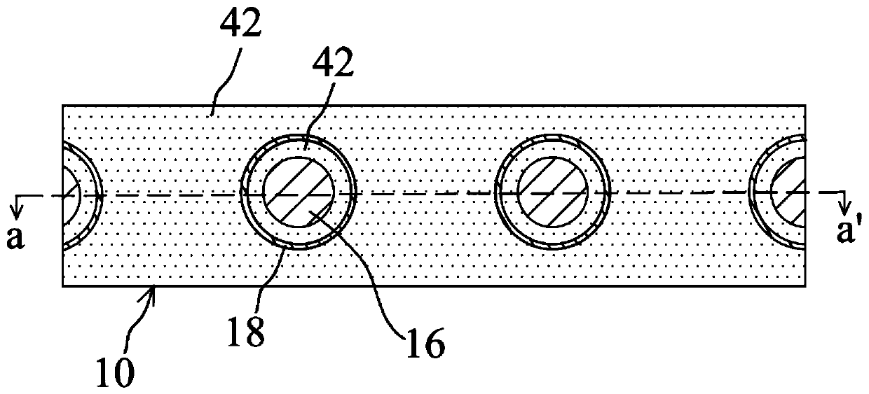
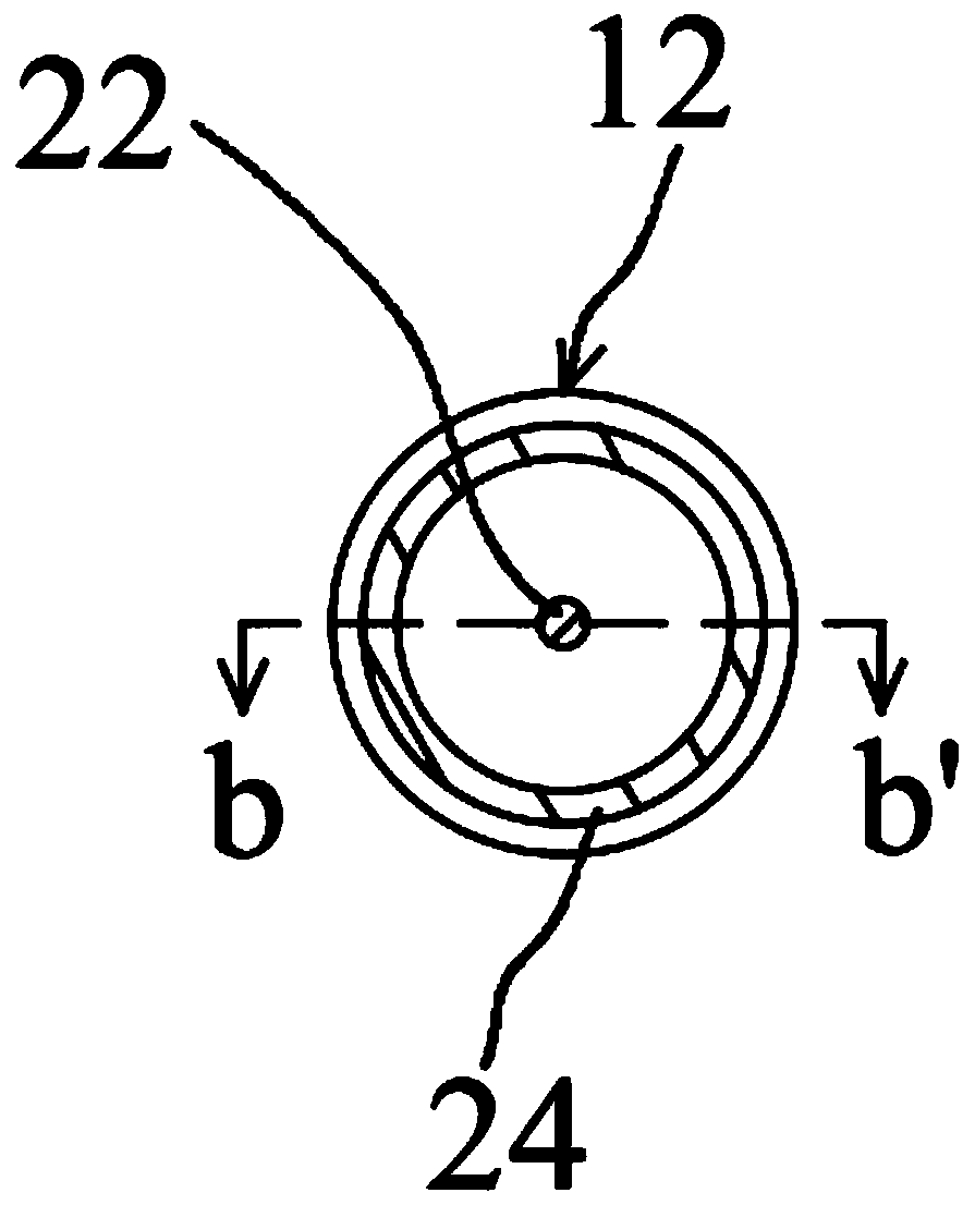
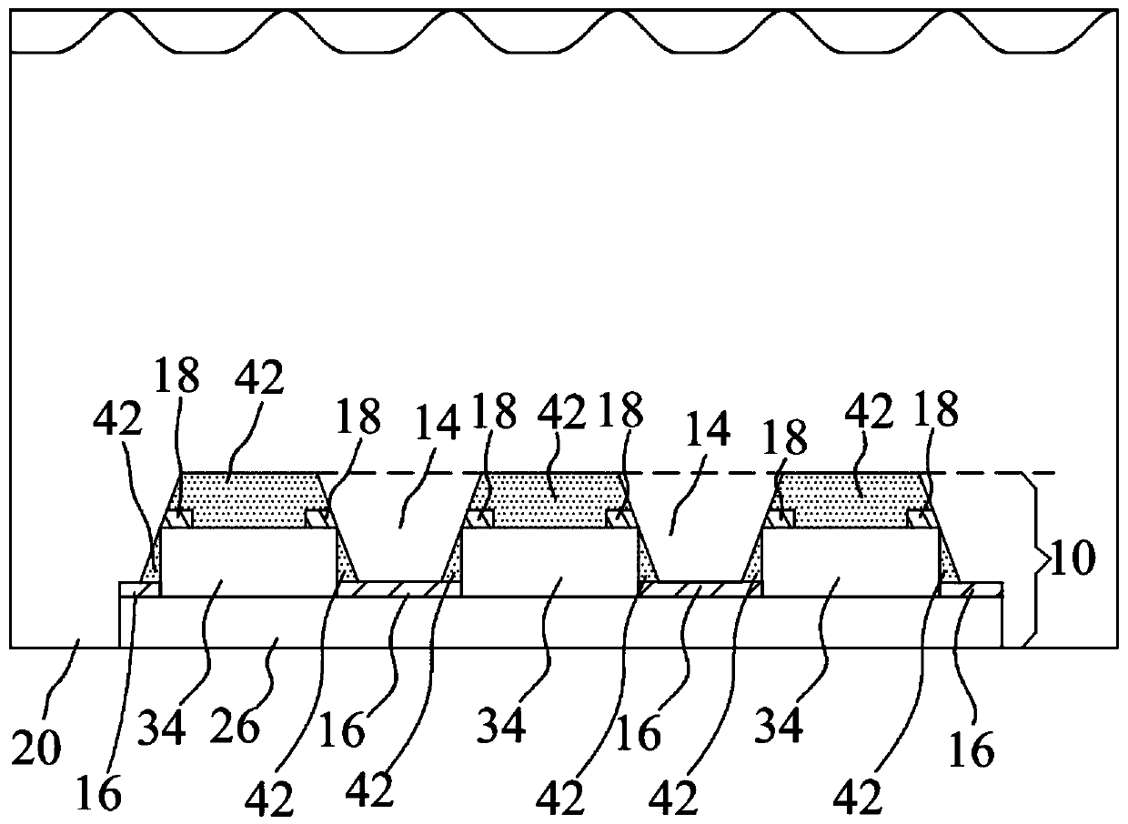
[0039] Embodiments of the present invention will be further explained in conjunction with the accompanying drawings below. Wherever possible, the same reference numerals represent the same or similar components throughout the drawings and description. In the drawings, the shape and thickness may be exaggerated for simplification and convenient labeling. It can be understood that the components not particularly shown in the drawings or described in the specification have forms known to those skilled in the art. Those skilled in the art can make various changes and modifications according to the content of the present invention.

[0040] When an element is referred to as being "on", it can generally mean that the element is directly on other elements, or there may be other elements present in between. Conversely, when an element is referred to as being "directly on" another element, it cannot have the other element in between. As used herein, the word "and / or" includes any co...


PUM


Abstract

The invention discloses a preparation method of a light emitting display. The preparation method comprises the steps of providing a packaging substrate, sinking the packaging substrate into a suspension, sinking a plurality of light emitting diodes into the suspension, and horizontally injecting the suspension, wherein a plurality of recesses are arranged at the top of the packaging substrate; each recess is provided with a first electrode region and a second electrode region in different height; the light emitting diodes are provided with planes and curved surfaces; the suspension has different flow rates on the planes and the curved surfaces of the light emitting diodes; all the light emitting diodes are respectively embedded into all the recesses according to the different flow rates; and each light emitting diode is electrically connected with the first electrode region and the second electrode region of the corresponding recess to form the light emitting display. According to thepreparation method, the packaging substrate and the light emitting diodes are assembled according to a bernoullis theorem on the premise that no damage is caused to the packaging substrate or the light emitting diodes.

Description

technical field [0001] The invention relates to a manufacturing method of an electronic device, and in particular to a manufacturing method of a light-emitting display. Background technique [0002] Fluid transfer from donor substrates / chips to large-area and / or conventional substrates for microfabricated electronic components, optoelectronic components, and subsystems offers new opportunities to expand the range of applications for electronic and optoelectronic devices. For example, light-emitting diode (LED) microstructures, such as rods, fins, or disks, can be fabricated on small-scale wafers to display pixel-level dimensions, and then transferred to large-panel glass substrates to form direct-emitting display. One traditional method of delivering these LED microstructures is through a pick-and-place process. However, for displays containing millions of pixels, such a process can take hours to complete and is therefore inefficient. [0003] Therefore, the present inven...

Claims


Application Information

Patent Timeline
Patent Type & Authority Applications(China)
IPC IPC(8): H01L33/00H01L27/15H01L33/62
CPCH01L25/0753H01L33/0095H01L33/62H01L27/156
Inventor 钟金峰
Owner INTERFACE TECH CHENGDU CO LTD
Why Eureka
Try Eureka