Micro-LED chip mass transfer method

A technology of LED chip and transfer method, which is applied in the manufacture of semiconductor devices, electrical components, semiconductor/solid-state devices, etc. It can solve the problems of insufficient precision, small micro-LED chips, and unsatisfactory yield, so as to achieve cost saving and high precision , The effect of simple and fast mass transfer

Active Publication Date: 2020-10-13
北京易美新创科技有限公司
View PDF3 Cites 0 Cited by
  • Summary
  • Abstract
  • Description
  • Claims
  • Application Information

AI Technical Summary

Problems solved by technology

Due to the small size and large quantity of micro-LED chips, it is the core technical problem faced in the industrialization process of micro-LEDs. There are technical problems such as insufficient transfer speed, insufficient precision, and unsatisfactory yield.

Method used


Image

  • Micro-LED chip mass transfer method
  • Micro-LED chip mass transfer method
  • Micro-LED chip mass transfer method

Examples


example 1

[0027] Example 1, the micro LED chip is a vertical chip

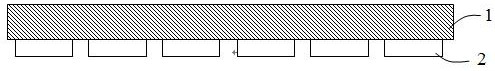
[0028] After the epitaxial structure is grown on the surface of the sapphire substrate, the device discrete grooves are etched in the epitaxial structure, and the distance between the centers of adjacent devices is 20 μm; the reflective layer material Ag, the isolation material TiW and the bonding material AuIn are sequentially deposited on the p surface of each device . Afterwards, perform a visual inspection and record the location of good products.

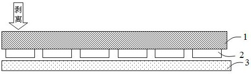
[0029] According to the results of visual inspection, use the laser lift-off method to peel off the good chip from the sapphire substrate and drop it on the adhesive film (temporary carrier); in the process of peeling the chip, arrange the fallen chips by moving the adhesive film In a square array, the distance between the centers of adjacent chips in the array is 20 μm*100 μm. Before the chip falls, the adhesive film is about 1mm away from the chip.

[0030] Use PDMS...

example 2

[0033] Example 2, the micro LED chip is a flip chip

[0034] After the epitaxial structure is grown on the surface of the sapphire substrate, the fabrication of the flip chip is completed and the chips are separated. The distance between the center points of adjacent chips in the horizontal and vertical directions is 100 μm*80 μm. After depositing the bonding material AuIn on the surface of the chip, perform a visual inspection and record the position of the good product.

[0035] According to the results of visual inspection, use the laser lift-off method to peel off the good chip from the sapphire substrate and drop it on the adhesive film (temporary carrier); in the process of peeling the chip, arrange the fallen chips by moving the adhesive film In a square array, the distance between the centers of adjacent chips in the array is 100 μm*80 μm. Before the chip falls, the adhesive film is about 1mm away from the chip.

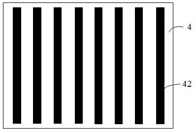
[0036] Use PDMS to make a stamp as shown in Figure 3,...


PUM


Abstract

The invention discloses a mass transfer method of micro LED chips, which comprises the steps of preparing micro LED chips on a growth substrate; equipping a temporary carrier with a sticky surface onone side; placing the chips on the surface of the growth substrate towards the temporary carrier, stripping the chips from the growth substrate and dropping the chips to the surface of the temporary carrier; preparing a stamp with a specific material, wherein the surface of the stamp is provided with regularly arranged bumps, and the surfaces of the bumps are sticky; placing the side with bumps ofthe stamp towards the surface of the temporary carrier, carrying out UV irradiating or heating on the temporary carrier, and enabling the bumps in the stamp to take down the corresponding chips fromthe surface of the temporary carrier; placing the stamp with the chips towards a target substrate, transferring the chips to the surface of the target substrate by means of bonding, and carrying out UV irradiating or heating on the bumps on the stamp so as to remove the stamp; and repeating the steps S2-S6 until the mass transfer of the chips is completed. The mass transfer method is simple and convenient, can achieve the purpose without complex equipment and saves a lot of cost.

Description

technical field [0001] The invention relates to the technical field of semiconductors, in particular to a method for mass transfer of micro-LED chips. Background technique [0002] Micro LED (Mini LED or Micro LED) is a drive circuit made of PCB, flexible PCB and CMOS / TFT integrated circuit technology after the traditional LED structure is thinned, miniaturized and matrixed. Addressable control and individually driven display technology. Due to the brightness, contrast, response time, viewing angle, resolution and other indicators of micro-LED technology are stronger than LCD and OLED technology, plus the advantages of self-illumination, simple structure, small size and energy saving, it has been widely accepted. focus on. [0003] After the micro-LED chips are fabricated, they need to be transferred to the driver circuit board to form an LED array, which is called Mass Transfer. Due to the small size and large quantity of micro-LED chips, it is the core technical problem...

Claims


Application Information

Patent Timeline
Patent Type & Authority Patents(China)
IPC IPC(8): H01L33/00H01L21/683H01L27/15
CPCH01L21/6835H01L27/156H01L33/0095H01L2221/68386
Inventor 刘国旭朱浩
Owner 北京易美新创科技有限公司
Why Eureka
Try Eureka