Luminescent device, manufacturing method thereof and display device

A technology of light-emitting devices and light-emitting units, applied in semiconductor/solid-state device manufacturing, semiconductor devices, electric solid-state devices, etc., can solve the problems of low outcoupling efficiency and light weakening of OLED devices, avoid waveguide effect and improve outcoupling efficiency Effect

Active Publication Date: 2019-06-18
BOE TECH GRP CO LTD
View PDF4 Cites 18 Cited by
  • Summary
  • Abstract
  • Description
  • Claims
  • Application Information

AI Technical Summary

Problems solved by technology

[0004] However, among the light emitted from the light-emitting unit into the thin-film packaging structure, the light with an incident angle within a certain range will be consumed by the waveguide effect in the thin-film packaging structure, so that the light emitted from the side of the thin-film packaging structure away from the light-emitting unit is weakened. , therefore, the outcoupling efficiency of the OLED device is low

Method used


Image

  • Luminescent device, manufacturing method thereof and display device
  • Luminescent device, manufacturing method thereof and display device
  • Luminescent device, manufacturing method thereof and display device

Examples


Embodiment Construction

[0052] In order to make the purpose, technical solution and advantages of the application clearer, the application will be further described in detail below in conjunction with the accompanying drawings. Apparently, the described embodiments are only some of the embodiments of the application, not all of them. Based on the embodiments in this application, all other embodiments obtained by persons of ordinary skill in the art without making creative efforts belong to the scope of protection of this application.

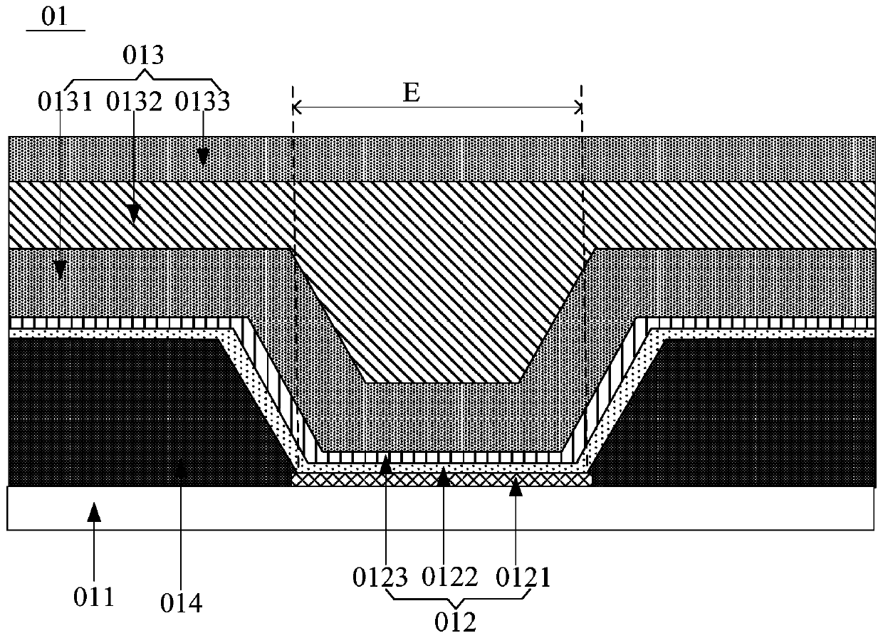
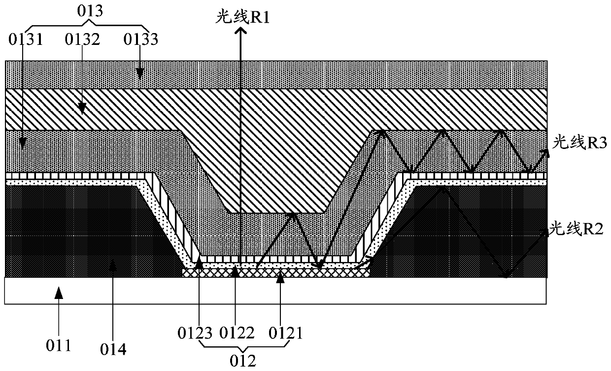
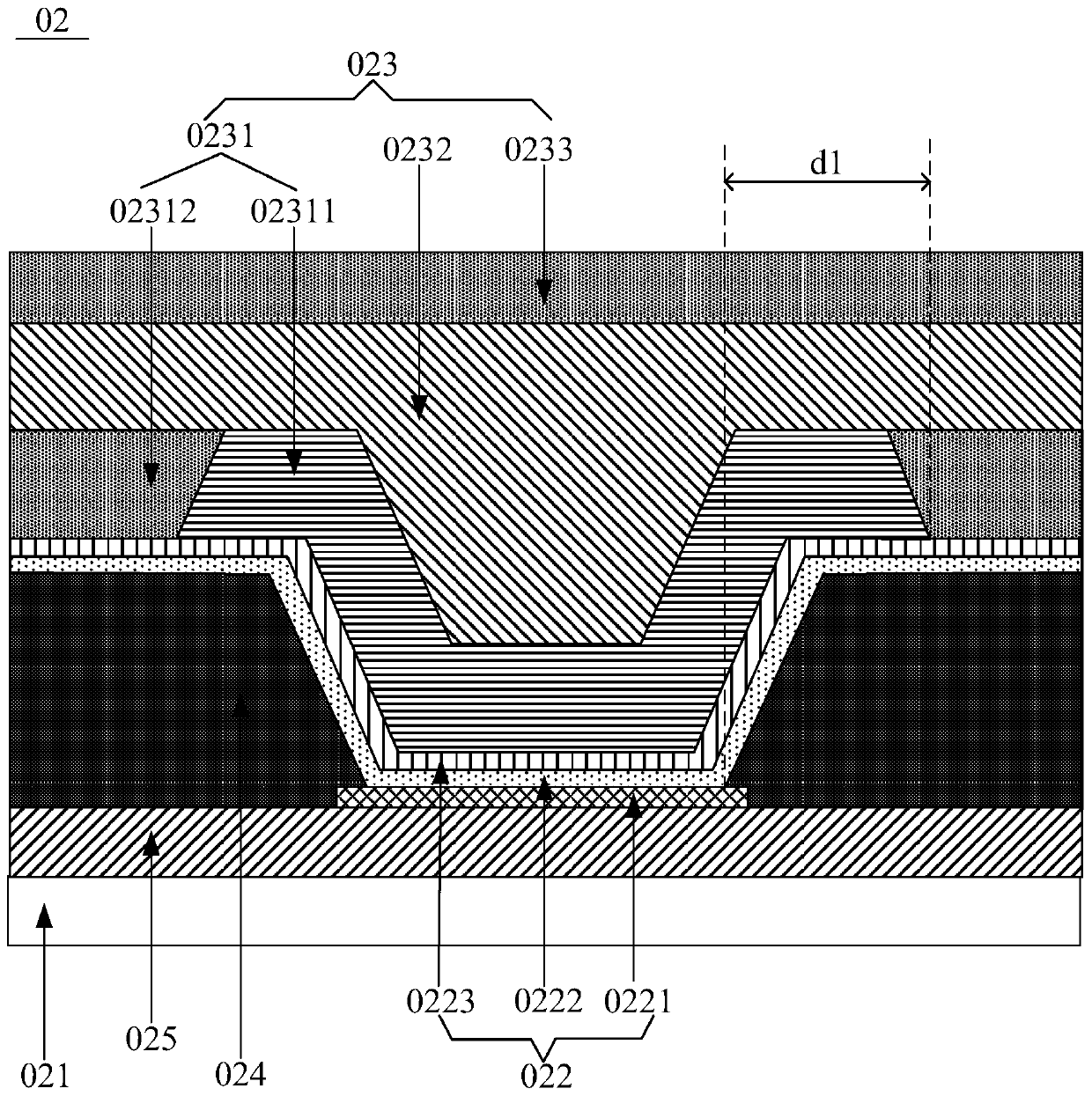
[0053] OLED devices are currently a research hotspot in the display industry. They usually include a light-emitting unit and a thin-film encapsulation structure for encapsulating the light-emitting unit. The existence of a thin-film encapsulation structure can prolong the service life of the OLED device while ensuring the flexibility of the OLED device. At present, the outcoupling efficiency of OLED devices is a hot and difficult point in industry research. Outcoupling ef...


PUM


Abstract

The invention discloses a luminescent device, a manufacturing method thereof and a display device, and belongs to the field of luminescent devices. The luminescent device comprises a substrate, a luminescent unit and a thin film packaging structure, wherein the luminescent unit is arranged on the substrate; the thin film packaging structure is arranged on the side, far away from the substrate, ofthe luminescent unit; the thin film packaging structure comprises at least one packaging film; a target packaging film in the at least one packaging film is provided with a first packaging part and asecond packaging part which is located at the same layer with the first packaging part and in contact with the first packaging part; the positive projection of the first packaging part on the substrate covers the positive projection of the luminescent unit on the substrate; and the refractive index of the first packaging part is smaller than the refractive index of the second packaging part. The luminescent device is beneficial for avoiding the light emitted by the luminescent unit from generating a waveguide effect on the thin film packaging structure, and is beneficial for improving the external coupling efficiency of the luminescent device. The invention is used for luminescent devices.

Description

technical field [0001] The present application relates to the field of light emitting devices, in particular to a light emitting device, a manufacturing method thereof, and a display device. Background technique [0002] Organic Light-Emitting Diode (English: Organic Light-Emitting Diode; abbreviation: OLED) device is an electroluminescent device, which has the advantages of low power consumption, self-luminescence, fast response, wide viewing angle and flexible display. hotspots. [0003] The OLED device includes a base substrate, a light-emitting unit arranged on the base substrate, and a thin-film packaging structure arranged on the side of the light-emitting unit away from the base substrate. When the OLED device is in operation, the light emitted by the light-emitting unit passes through the thin-film package The side of the structure close to the light-emitting unit is injected into the thin-film packaging structure, and is emitted from the thin-film packaging structu...

Claims


Application Information

Patent Timeline
Patent Type & Authority Applications(China)
IPC IPC(8): H01L51/52H01L51/56
CPCH10K50/858H10K50/856H10K50/844H10K71/00
Inventor 高昊王涛
Owner BOE TECH GRP CO LTD
Why Eureka
Try Eureka