A kind of oled structure size optimization design method and equipment

An optimized design and structural layer technology, applied in CAD circuit design, computer aided design, calculation, etc., to achieve the effect of easy operation, improved efficiency, and simple principle

Active Publication Date: 2020-11-24
武汉宇微光学软件有限公司
View PDF2 Cites 0 Cited by
  • Summary
  • Abstract
  • Description
  • Claims
  • Application Information

AI Technical Summary

Problems solved by technology

[0009] In view of the above defects or improvement needs of the prior art, the present invention provides an OLED structure optimization design method and equipment, the purpose of which is to take the optical characteristic parameters of anisotropic materials into consideration when establishing a mathematical model, and calculate The outcoupling efficiency of OLEDs with different structural sizes, thus solving the structural optimization problem of OLEDs containing anisotropic materials

Method used


Image

  • A kind of oled structure size optimization design method and equipment
  • A kind of oled structure size optimization design method and equipment
  • A kind of oled structure size optimization design method and equipment

Examples


Embodiment Construction

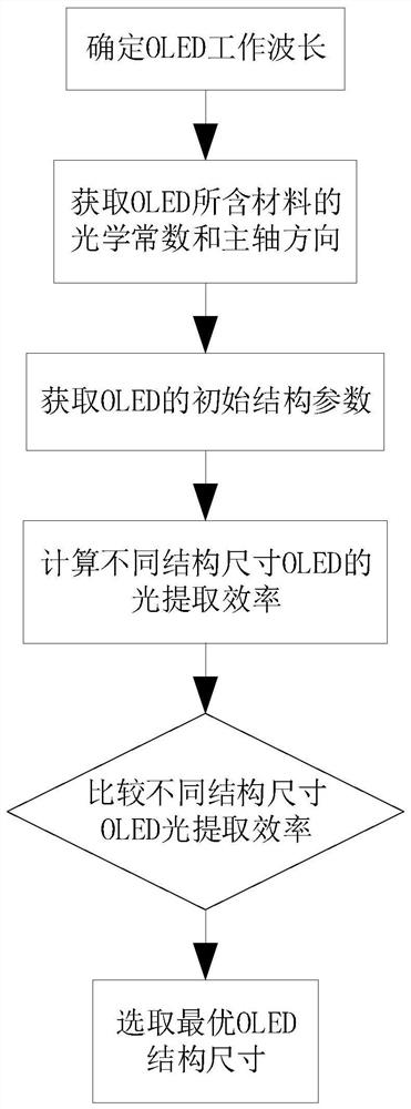
[0053] In order to make the object, technical solution and advantages of the present invention clearer, the present invention will be further described in detail below in conjunction with the accompanying drawings and embodiments. It should be understood that the specific embodiments described here are only used to explain the present invention, not to limit the present invention. In addition, the technical features involved in the various embodiments of the present invention described below can be combined with each other as long as they do not constitute a conflict with each other.

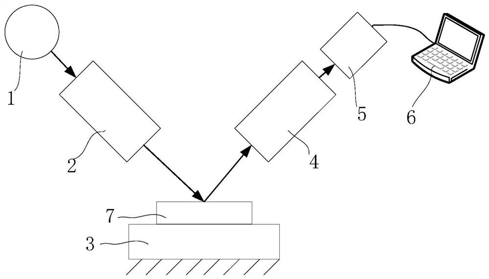
[0054] In order to more clearly illustrate the implementation process of the OLED structure optimization calculation method described in the present invention, the Muller matrix ellipsometer is preferably used in this example to detect the optical constants and the main axis direction of the materials contained in the OLED. The specific process is as follows figure 1 shown. figure 2 It is a sc...


PUM

PropertyMeasurementUnit
refractive indexaaaaaaaaaa
thicknessaaaaaaaaaa
thicknessaaaaaaaaaa

Abstract

The invention discloses an OLED structure optimization design method and device and belongs to OLED field. The method includes the following steps: step 1, determining the working wavelength lambda ofOLED, the optical constant of each layer material of OLED, the initial design thickness value of each layer material of OLED and the azimuth of the main axis of anisotropic material in OLED, theta and psi; step 2, establishing the multi-layer stack optical model of OLED based on the parameters identified in step 1 and adjusting the thickness of cathode, cathode finish layer, luminous layer, holetransport layer, hole injection layer, anode and the layer to be optimized in the substrate. The simulation test is conducted to obtain the external coupling efficiency of OLED at different structurethicknesses and determine the maximum structural thickness of external coupling efficiency. The device is used to executive the above method. The method has the advantages of simple principle and easy-to-operate and can realize the simulation optimization calculation of OLED structure dimension.

Description

technical field [0001] The invention belongs to the field of organic light-emitting diodes (OLEDs), and more specifically relates to an OLED structure size optimization design method and equipment, which are suitable for optimizing the design of the OLED structure size to improve its outcoupling efficiency. Background technique [0002] Since the 1960s when Pope and his collaborators performed voltage experiments on single crystal anthracene and discovered the phenomenon of blue photoluminescence (Journal of Chemical Physics, 1963, 38(8): 2042-2043), scientists have gradually begun to pay attention to organic electroluminescence. Research on luminescent materials and devices. Organic electroluminescence refers to the phenomenon that organic materials emit light under the excitation of electric current or electric field, and devices made according to this principle are called organic light emitting diodes (Organic light emitting diode, OLED). [0003] OLED refers to a light-...

Claims


Application Information

Patent Timeline
Patent Type & Authority Patents(China)
IPC IPC(8): G06F30/398H01L27/02
CPCG06F30/39G06F30/398H01L27/0203
Inventor 谷洪刚赵雪楠刘世元柯贤华
Owner 武汉宇微光学软件有限公司
Why Eureka
Try Eureka