

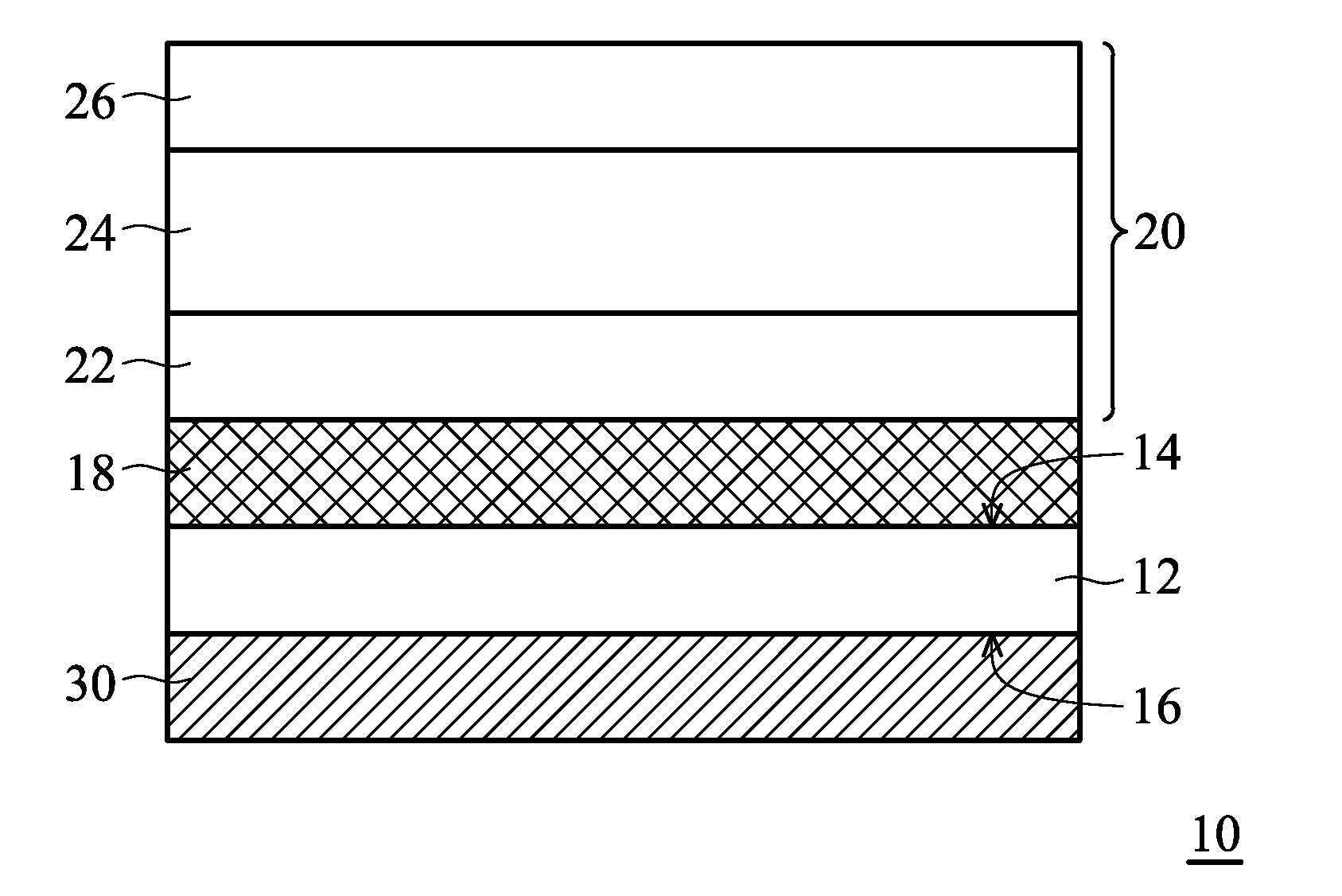
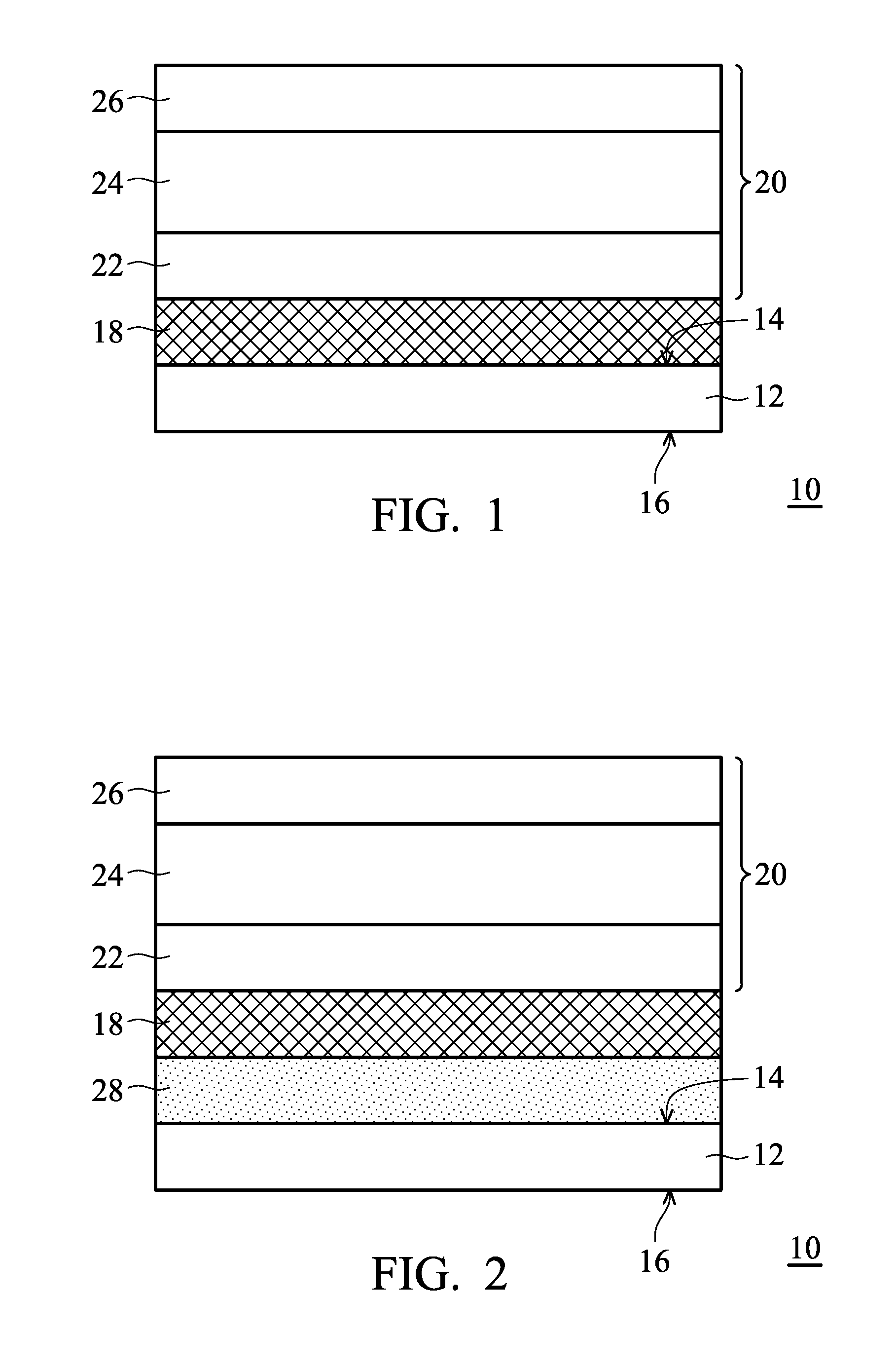
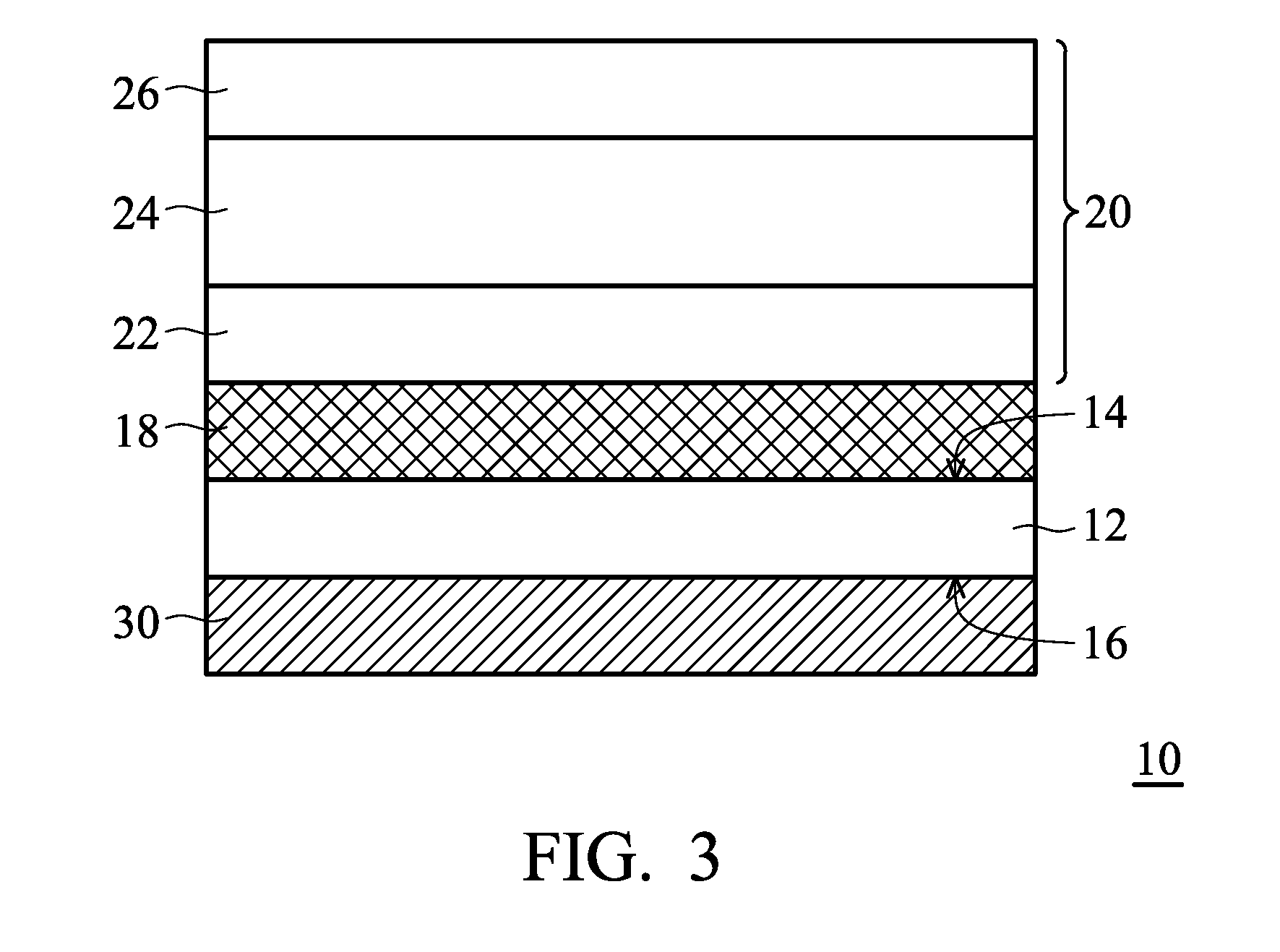
Optical device structures with the light outcoupling layers
a technology of optical devices and light outcoupling layers, which is applied in the direction of light and heating equipment, transportation and packaging, synthetic resin layered products, etc., can solve the problems of 20% of light to be emitted from the front of the device, and the inability of fabricated ito films to sinter (annealing) at a high temperature, so as to reduce the surface resistance value and refraction index of the upper conductive films. , the effect of efficient improvement of ligh
- Summary
- Abstract
- Description
- Claims
- Application Information
AI Technical Summary
Benefits of technology
Problems solved by technology
Method used
Image

Examples
example 1
Preparation and Physical Properties of the Polyimide (PI-1)
[0027]A polyimide comprising 2,2-bis[4-(4-aminophenoxy)phenyl]propane A and bicyclo[2,2,2]oct-7-ene-2,3,5,6-tetracarboxylic dianhydride B with a composition ratio of 5:5 was prepared. First, 82.7 g of 2,2-bis[4-(4-aminophenoxy)phenyl]propane A, 50 g of bicyclo[2,2,2]oct-7-ene-2,3,5,6-tetracarboxylic dianhydride B and 530.8 g of m-cresol were added to a 2 L glass reactor and reacted with electric stirring under 220° C. for 4 hours to form a polyimide solution with a solid content of 20%. The polyimide solution was then re-precipitated with methanol. After drying, filamentous polyimide (PI) was obtained. The filamentous polyimide (PI) was dissolved by dimethyl acetamide to prepare a polyimide (PI-1) solution with a solid content of 15%.
[0028]In this example, the b value (yellow value) of the prepared polyimide (PI-1) was 2.37.
example 2
Preparation and Physical Properties of the Polyimide (PI-2)
[0029]A polyimide comprising 2,2-bis[4-(4-aminophenoxy)phenyl]propane A, 4,4-diaminodiphenyl ether B and pyromellitic dianhydride C with a composition ratio of 3:7:10 was prepared. First, 28.2 g of 2,2-bis[4-(4-aminophenoxy)phenyl]propane A, 32.1 g of 4,4-diaminodiphenyl ether B, 50 g of pyromellitic dianhydride C and 441.4 g of m-cresol were added to a 2 L glass reactor and reacted with electric stirring under 220° C. for 4 hours to form a polyimide solution with a solid content of 20%. The polyimide solution was then re-precipitated with methanol. After drying, filamentous polyimide (PI) was obtained. The filamentous polyimide (PI) was dissolved by dimethyl acetamide to prepare a polyimide (PI-2) solution with a solid content of 15%.
[0030]In this example, the b value (yellow value) of the prepared polyimide (PI-2) was 1.95.
example 3
Preparation and Physical Properties of the Polyimide (PI-3)
[0031]A polyimide comprising 2,2-bis[4-(4-aminophenoxy)phenyl]propane A and bicyclo[2,2,2]oct-7-ene-2,3,5,6-tetracarboxylic dianhydride B with a composition ratio of 5:5 was prepared. First, 82.7 g of 2,2-bis[4-(4-aminophenoxy)phenyl]propane A, 50 g of bicyclo[2,2,2]oct-7-ene-2,3,5,6-tetracarboxylic dianhydride B and 530.8 g of m-cresol were added to a 2 L glass reactor and reacted with electric stirring under 220° C. for 4 hours to form a polyimide solution with a solid content of 20%. The polyimide solution was then re-precipitated with methanol. After drying, filamentous polyimide (PI) was obtained. The filamentous polyimide (PI) was dissolved by dimethyl acetamide to prepare a polyimide (PI-3) solution with a solid content of 15%.
[0032]In this example, the b value (yellow value) of the prepared polyimide (PI-3) was 2.37.
PUM
| Property | Measurement | Unit |
|---|---|---|
| thickness | aaaaa | aaaaa |
| thickness | aaaaa | aaaaa |
| weight | aaaaa | aaaaa |
Abstract
Description
Claims
Application Information