Metallic anode treated by carbon tetrafluoride plasma for organic light emitting device

a technology of carbon tetrafluoride and organic light, which is applied in the direction of basic electric elements, semiconductor devices, electrical equipment, etc., can solve the problems of 80% of generated light still unavailable for viewing, complicated structure, and high cost of fabrication, so as to improve the ability of carrier, facilitate microcavity fabrication, and simplify the effect of structur

Inactive Publication Date: 2015-10-20
THE HONG KONG UNIV OF SCI & TECH
View PDF24 Cites 0 Cited by
  • Summary
  • Abstract
  • Description
  • Claims
  • Application Information

AI Technical Summary

Benefits of technology

[0016]The present invention provides a metallic electrode, including Ag or Au or the alloy thereof, to function as the anode in OLEDs. The present invention modifies the surface of the metallic anode with CF4 plasma to enhance the ability of carrier, especially the hole injection into the emissive unit. The present invention also provides an easily fabricated microcavity OLED using the metallic electrode as a reflective mirror.
[0017]Microcavity OLEDs using metallic anode are simpler in structure and easier to fabricate than those using a QWS, with elimination of: (1) deposition of multilayer dielectric stacks; and (2) the need for a separate transparent conductive anode. The microcavity OLED devices using this metallic electrode as an anode have substantially improved outcoupling efficiency, compared with that of a conventional bottom emitting device without a microcavity.

Problems solved by technology

Although conventional bottom LED engineering is rather mature, in general up to 80% of generated light is still unavailable for viewing, due to the losses in waveguiding modes, in the glass, ITO and organic layers and in surface plasmon modes in the metallic cathode.
A QWS, however, is a complicated structure and expensive to fabricate.
In addition, a separated transparent electrode layer, usually an Indium Tin Oxide (ITO), is layered between the QWS and the organic layers, which further complicates the structure.

Method used


Image

  • Metallic anode treated by carbon tetrafluoride plasma for organic light emitting device
  • Metallic anode treated by carbon tetrafluoride plasma for organic light emitting device
  • Metallic anode treated by carbon tetrafluoride plasma for organic light emitting device

Examples


example 1

[0037]A comparative device (1A) and a device (1B) of present invention each having an Ag anode layer were made. The Ag anodes were deposited on a 1.1 thick bare glass sheet with thickness of 60 nm. The Ag anode of the device 1B was treated by CF4 plasma in a plasma treatment chamber in accordance with the present invention. Then the following layers were deposited in the following manner from a heated boat in the vacuum chamber under a vacuum less than 1×10⁻⁶ torr:

(1) a hole-transporting layer, consisting of 140 nm NPB; and

(2) a cathode layer, consisting of 110 nm Al.

[0038]FIG. 4 shows the current voltage relationships of the devices described in Example 1A and Example 1B. The figure shows that when the Ag anode is modified by the CF4 plasma, the device shows fast-rising J-V curve and low operation driving voltage, as compared to those obtained from comparative device 1A.

example 2

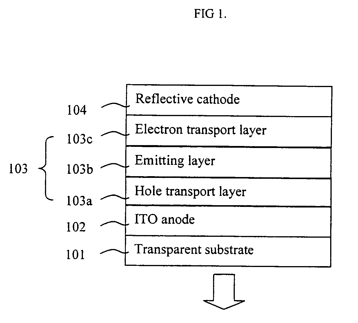
[0039]A conventional bottom emitting OLED was made using ITO as the transparent anode. After routine cleaning, the ITO was treated with CF4 plasma in a plasma treatment chamber. Then, the following layers were deposited in the following sequence from a heated boat in the vacuum chamber under a vacuum of less than 1×10⁻⁶ torr:

(1) a hole-transporting layer, of 70 nm NPB;

(2) a light emitting layer, of 30 nm Alq doped with 1% C545T;

(3) a electron transport layer, of 30 nm Alq; and

(4) a cathode layer, of 1 nm LiF covered with 110 nm Al.

[0040]The device structure is Glass / ITO (75 nm) / NPB (70 nm) / Alq: 1% C545T (30 nm) / Alq (30 nm) / LiF (1 nm) / Al (110 nm).

example 3

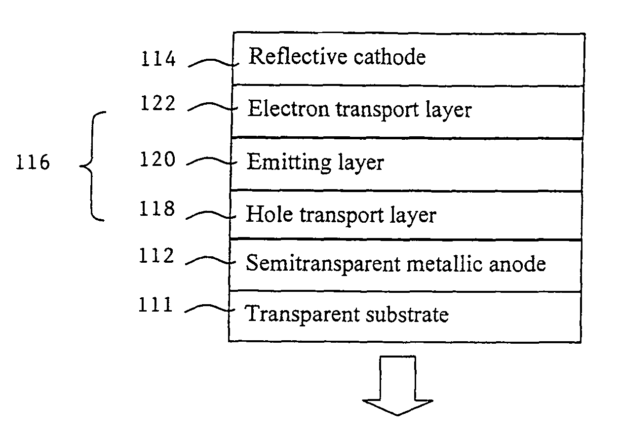
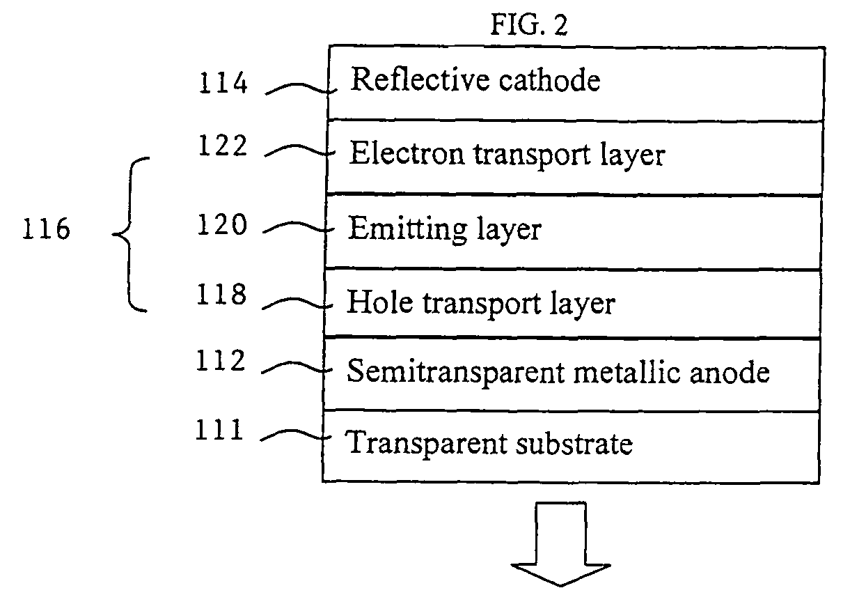
[0041]A series of bottom emitting OLEDs of the present invention (devices 3A, 3B, 3C, 3D, and 3E), each having an Ag anode were made. The Ag anodes were deposited on a 1.1 nm thick bare glass sheet with thickness varying from 15 nm to 50 nm. The Ag anode surface was treated by CF4 plasma in a plasma treatment chamber. Then the following layers were deposited in the following sequence from a heated boat in the vacuum chamber under a vacuum less than 1×10⁻⁶ torr:

(1) a hole-transporting layer, of 50 nm NPB;

(2) a light emitting layer, of 24 nm Alq doped with 1% C545T;

(3) a electron transport layer, of 24 nm Alq; and

(4) a cathode layer, of 1 nm LiF covered with 110 nm Al.

[0042]The device structure is Glass / Ag (x nm) / NPB (50 nm) / Alq: 1% C545T (24 nm) / Alq (30 nm) / LiF (1 nm) / Al (110 nm).

[0043]The results of Examples 2 and 3 are listed in Table 1 attached hereto. Devices having a semitransparent Ag anode of present invention demonstrate a luminance efficiency that is higher than that of the ...


PUM


Abstract

The invention provides an organic light emitting diode (OLED), having a substrate, an anode layer of silver or gold, wherein the anode layer is treated with CF4 plasma to enhance the hole injection of the semitransparent anode layer.

Description

CROSS-REFERENCE TO RELATED APPLICATION[0001]This application claims the benefit of U.S. Provisional Patent Application Ser. No. 60 / 711,803, filed Aug. 29, 2005, the entire contents of which is included by reference herein.FIELD OF THE INVENTION[0002]The present invention relates to Organic Light Emitting Diode (OLED) displays. In particular, it provides microcavity organic light emitting diodes that use a metallic electrode as an anode and provides methods to fabricate such devices.BACKGROUND OF THE INVENTION[0003]One important parameter of an OLED device is the outcoupling efficiency, which is the fraction of the internally emitted photons that actually escape outside. Although conventional bottom LED engineering is rather mature, in general up to 80% of generated light is still unavailable for viewing, due to the losses in waveguiding modes, in the glass, ITO and organic layers and in surface plasmon modes in the metallic cathode.[0004]One method that potentially can enhance the l...

Claims


Application Information

Patent Timeline
Patent Type & Authority Patents(United States)
IPC IPC(8): H01L51/52
CPCH01L51/5265H01L51/5206H10K50/81H10K50/818H10K50/852
Inventor KWOK, HOI SINGWONG, MANPENG, HUAJUNSUN, JIAXIN
Owner THE HONG KONG UNIV OF SCI & TECH
Why Eureka
Try Eureka