A method for testing an artificial intelligence module on a system chip and a system chip

A system-on-chip, chip technology, applied in computing models, biological neural network models, instruments, etc., can solve problems such as difficulty in adapting to the large bandwidth requirements of AI modules and long testing time.

Active Publication Date: 2019-06-21
HERCULES MICROELECTRONICS CO LTD
View PDF9 Cites 5 Cited by
  • Summary
  • Abstract
  • Description
  • Claims
  • Application Information

AI Technical Summary

Problems solved by technology

[0003] Artificial intelligence modules generally mainly perform data calculation functions, usually require a large number of test incentives, and the test time is also long
[0004] In addition, the artificial intelligence AI module is accessed by the processor through the bus, and the bus has a certain bandwidth limit. Such an architecture is difficult to meet the large bandwidth requirements of the AI ​​module.

Method used


Image

  • A method for testing an artificial intelligence module on a system chip and a system chip
  • A method for testing an artificial intelligence module on a system chip and a system chip
  • A method for testing an artificial intelligence module on a system chip and a system chip

Examples


Embodiment Construction

[0023] In order to express the technical solutions and advantages of the embodiments of the present invention more clearly, the technical solutions of the present invention will be further described in detail below with reference to the drawings and embodiments.

[0024] In the description of this application, the terms "center", "upper", "lower", "front", "rear", "left", "right", "east", "south", "west", "north ", "vertical", "horizontal", "top", "bottom", "inner", "outer" and other indicated orientations or positional relationships are based on the orientations or positional relationships shown in the drawings, and are only for the convenience of description The present application and simplified descriptions do not indicate or imply that the device or element referred to must have a particular orientation, be constructed and operate in a particular orientation, and thus should not be construed as limiting the present application.

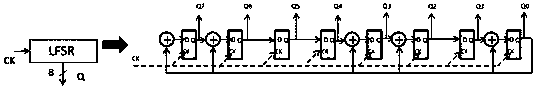
[0025] figure 1 It is a schematic circuit...


PUM


Abstract

The invention discloses a method for testing an artificial intelligence module on a system chip and a system chip. In an embodiment, a system chip comprises: an AI module comprising a plurality of processing units, each of the plurality of processing units completing a logical and / or multiply-add operation; Wherein the AI module is provided with: a self-test circuit; an FPGA module which is communicated with the AI module through the interface module so as to provide data for the AI module or receive an operation result of the AI module; And the JTAG interface which is used for starting the self-test circuit according to the instruction so as to test each processing unit of the AI module. And a self-test circuit is arranged in the AI module, so that the test work of the AI module can be greatly simplified.

Description

technical field [0001] The invention relates to the technical field of integrated circuits, in particular to a method for testing an artificial intelligence module on a system chip and the system chip. Background technique [0002] In recent years, artificial intelligence has ushered in a wave of development. Artificial intelligence is a discipline that studies the use of computers to simulate certain thinking processes and intelligent behaviors (such as learning, reasoning, thinking, planning, etc.) Higher-level applications can be realized. [0003] Artificial intelligence modules generally mainly perform data calculation functions, which usually require a large number of test stimuli and the test time is relatively long. [0004] In addition, the artificial intelligence AI module is accessed by the processor through the bus, and the bus has a certain bandwidth limit. Such an architecture is difficult to meet the large bandwidth requirements of the AI ​​module. Content...

Claims


Application Information

Patent Timeline
Patent Type & Authority Applications(China)
IPC IPC(8): G06N20/00G06N3/063
Inventor 连荣椿王海力马明
Owner HERCULES MICROELECTRONICS CO LTD
Why Eureka
Try Eureka