TFT panel and testing method
A test method and panel technology, applied in semiconductor/solid-state device test/measurement, electrical measurement, measurement device, etc., can solve the problems of high material cost and production capacity cost, high test fixture requirements, low test success rate, etc. The effect of reducing material cost and production capacity cost and improving test success rate
- Summary
- Abstract
- Description
- Claims
- Application Information
AI Technical Summary
Problems solved by technology
Method used
Image

Examples
Embodiment 1
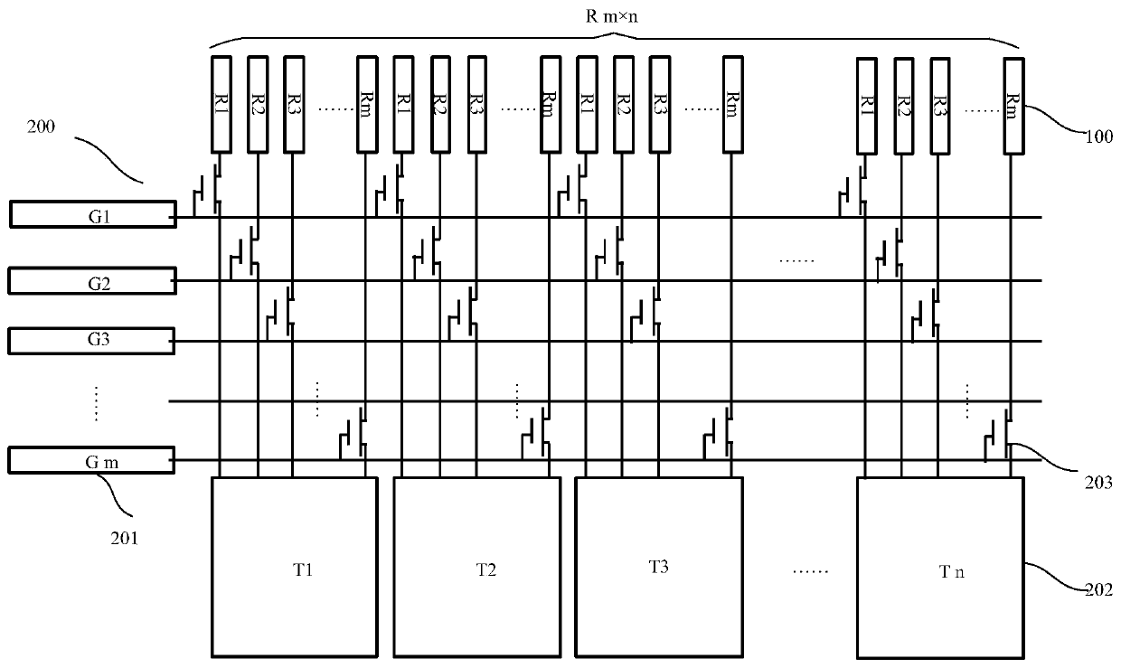
[0034] This embodiment provides a TFT panel, and the TFT panel includes:
[0035] m×n bonding pads, wherein both m and n are natural numbers greater than or equal to 1, and the m×n bonding pads are correspondingly arranged and electrically connected to the TFT units in the TFT active area;
[0036] TFT test area, the TFT test area includes m drive pads, n test pads and m×n TFT devices, wherein the m×n TFT devices are divided into n groups, and each group includes m For the TFT devices, the m TFT devices in each group are respectively electrically connected to the m driving pads and the m bonding pads, and the m TFT devices in each group are connected to n One of the test pads is electrically connected to one of the test pads.
[0037] In the TFT panel in this embodiment, by integrating a TFT test area including m drive pads, n test pads and m×n TFT devices on the TFT panel, the pad spacing required for testing is increased, thereby Reduce the requirements for test equipment ...
Embodiment 2
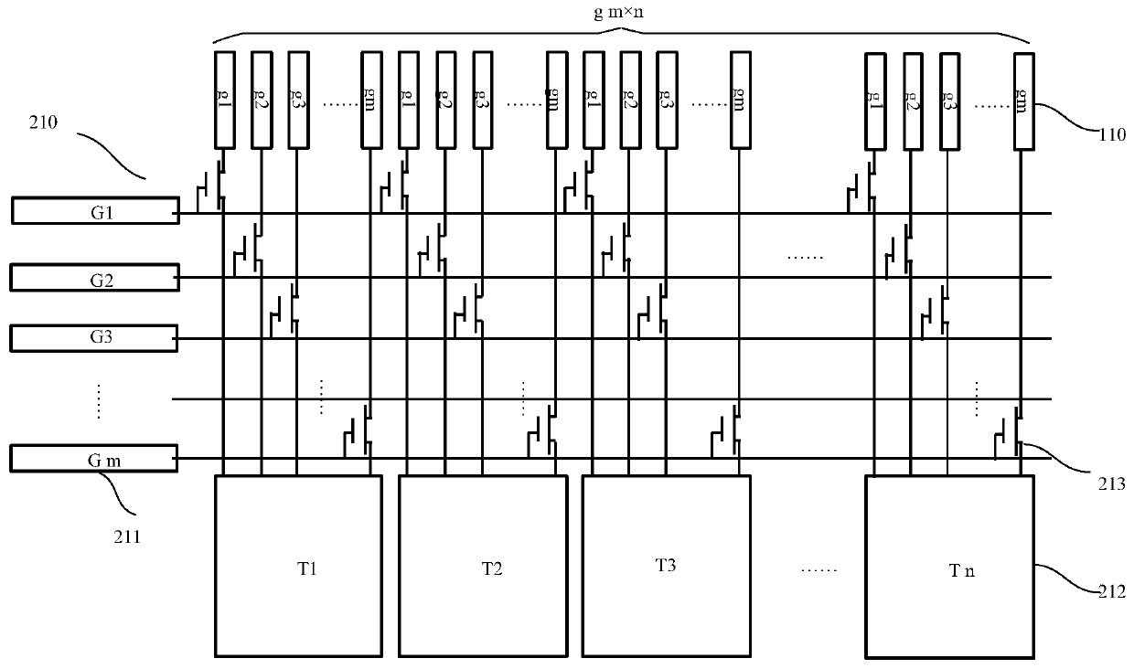
[0048] Such as figure 2 As shown, in order to further explain the solution of the present invention, this embodiment also provides another TFT panel. Compared with Embodiment 1, the difference is that the bonding pad 110 in this embodiment is located on the driving side of the TFT panel Bonding pads, it is only necessary to convert the high-precision reading-side bonding pads in Embodiment 1 into driving-side bonding pads in the TFT panel, wherein the function of the bonding pads is determined by Read becomes drive, which is still controlled by the low-precision drive pad 211 .
[0049] Specifically, in this embodiment, the TFT panel includes: m×n bonding pads 110 and TFT test areas 210 . Where m and n are both natural numbers greater than or equal to 1, and the m×n bonding pads 110 are driving side bonding pads located in the TFT panel, that is, the bonding pads 110 include n g1 ~gm, and corresponding to the TFT unit (not shown) in the TFT effective area; the TFT test area...
Embodiment 3
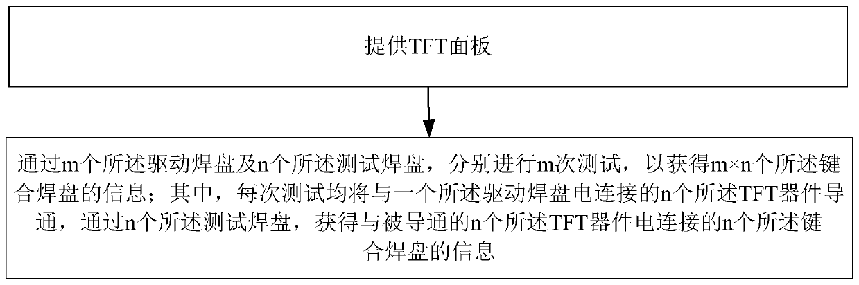
[0053] Such as image 3 , the present embodiment provides a method for testing a TFT panel, comprising the following steps:
[0054] Provide any one of the above-mentioned TFT panels;
[0055] Through the m driving pads and the n testing pads, respectively perform m tests to obtain the information of the m×n bonding pads; wherein, each test will be related to one of the driving pads The n TFT devices electrically connected to the pads are turned on, and the information of the n bonding pads electrically connected to the n TFT devices that are turned on is obtained through the n test pads.
[0056] Specifically, this embodiment integrates a TFT test area including m drive pads, n test pads, and m×n TFT devices on the TFT panel, so that the number m+n of pads required for testing is smaller than that of the TFT panel The number of bonding pads in m×n, so that the pad spacing required for the test is greater than the bonding pad spacing in the TFT panel; when testing the TFT pa...
PUM
 Abstract
Description
Claims
Application Information
 - R&D
- Intellectual Property
- Life Sciences
- Materials
- Tech Scout
- Unparalleled Data Quality
- Higher Quality Content
- 60% Fewer Hallucinations
Browse by: Latest US Patents, China's latest patents, Technical Efficacy Thesaurus, Application Domain, Technology Topic, Popular Technical Reports.
© 2025 PatSnap. All rights reserved.Legal|Privacy policy|Modern Slavery Act Transparency Statement|Sitemap|About US| Contact US: help@patsnap.com