

Electron transport material, preparation method thereof and light emitting diode
An electron transport material and light-emitting diode technology, applied in the field of materials, can solve the problems affecting the luminous efficiency and service life of the device, and the uneven hole-electron charge injection, etc., achieve excellent solution processing performance, increase the hole-electron recombination rate, good The effect of solubility
- Summary
- Abstract
- Description
- Claims
- Application Information
AI Technical Summary
Problems solved by technology
Method used
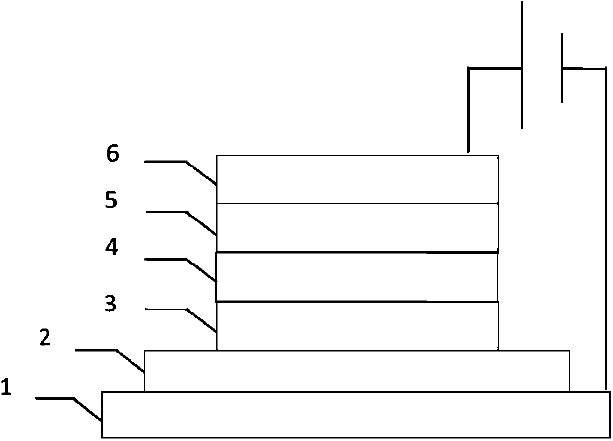
Image

Examples
preparation example Construction
[0025] Correspondingly, an embodiment of the present invention is also a preparation method of an electron transport material, comprising the following steps:
[0026] S01: Provide metal oxide nanoparticles and an alkoxysilane coupling agent containing amino groups at the end of the non-alkoxy carbon chain, dissolve the metal oxide nanoparticles and the silane coupling agent in an organic solvent, and heat Process to obtain the first solution;
[0027] S02: providing MMA monomers and catalysts, adding the MMA monomers and the catalysts to the first solution, and performing an acylation reaction to obtain a second solution;
[0028] S03: providing an azo initiator, adding the initiator into the second solution to carry out a polymerization reaction to obtain the electron transport material.
[0029] The preparation method of the electron transport material provided by the embodiment of the present invention can obtain the electron transport material with adjustable electron in...
Embodiment 1
[0057] A preparation method of an electron transport material, utilizing zinc oxide nano particle powder, KH550 silane coupling agent, MMA monomer, AIBN initiator, xylene, etc. to prepare a ZnO electron transport layer, comprising the following steps:
[0058] Disperse zinc oxide nanoparticles with a particle size range of 5-30nm in xylene (10-100mg / mL) and keep stirring, heat to 160°C under the protection of argon atmosphere, and then add 2-4mL of KH550 as silane coupling agent, and keep warm for 3 hours.
[0059] After heating, the solution was cooled to room temperature, centrifuged, washed with acetone and ethanol, dried to obtain silanized zinc oxide nanoparticles, and redispersed in xylene, maintaining high-speed stirring. Inject 2-8mL of MMA and 10-100mg of sodium ethoxide catalyst into the xylene solution, stir evenly, heat to 90°C and keep it warm for 1 hour, then inject 10-100mg of AIBN, keep it warm for 1 hour and then cool down to room temperature. Subsequently, t...
Embodiment 2
[0061] A preparation method for electron transport materials, using titanium dioxide nanoparticle powder, KH550 silane coupling agent, MMA monomer, AIBME initiator, toluene, etc. to prepare TiO 2 Electron transport layer, comprising the following steps:
[0062] Take titanium dioxide nanoparticles with a particle size range of 5-30nm and disperse them in toluene (10-100mg / mL) and keep stirring, heat to 150°C under the protection of argon atmosphere, then add 2-4mL of KH550 as a silane coupling agent, And keep warm for 3 hours.
[0063]After heating, the solution was cooled to room temperature, centrifuged, washed with acetone and ethanol, dried to obtain silanized titanium dioxide nanoparticles, and redispersed in toluene, maintaining high-speed stirring. Inject 4-8mL of MMA and 10-100mg of PCC condensing agent into the toluene solution, stir evenly, heat to 90°C and keep it warm for 1 hour, then inject 10-100mg of AIBME into the toluene solution, keep it warm for 1 hour and ...
PUM
| Property | Measurement | Unit |
|---|---|---|
| particle diameter | aaaaa | aaaaa |
Abstract
Description
Claims
Application Information