Wafer bonding process for transferring multiple wafers at one time

A chip and solid crystal technology, which is applied in semiconductor/solid-state device manufacturing, electrical components, circuits, etc., can solve the problem of low transfer efficiency, achieve the effect of improving transfer efficiency and reducing the time required

Inactive Publication Date: 2019-06-28
SHENZHEN FONTAI IND TECH CO LTD
View PDF8 Cites 8 Cited by
  • Summary
  • Abstract
  • Description
  • Claims
  • Application Information

AI Technical Summary

Problems solved by technology

[0003] The existing crystal-bonding process can usually only transfer one wafer (or chip) at a time, and the transfer efficiency is relatively low. The present invention solves this problem

Method used


Image

  • Wafer bonding process for transferring multiple wafers at one time
  • Wafer bonding process for transferring multiple wafers at one time
  • Wafer bonding process for transferring multiple wafers at one time

Examples


Embodiment Construction

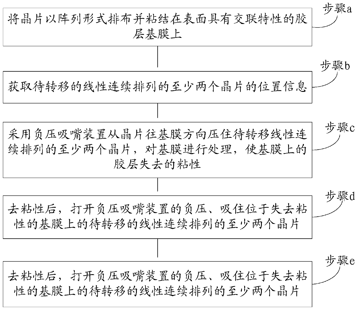
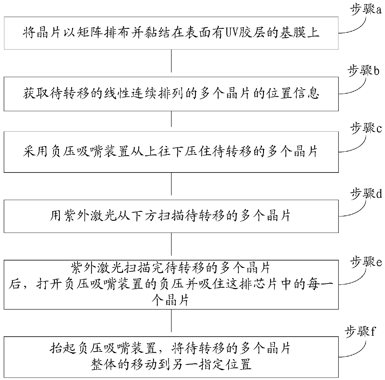
[0038] refer to figure 1 , the invention discloses a crystal-bonding process for transferring a plurality of wafers at a time. The wafers mainly refer to tiny chips, and these tiny chips are in an array (such as Figure 6 shown) are arranged on a base film (such as PET film or other types of films) with UV glue to form a dot matrix of chips. This base film with UV glue layer can be called a UV adhesive tape.

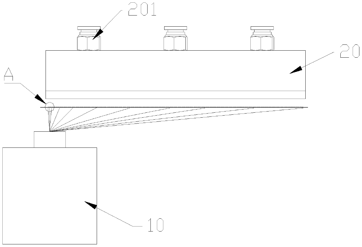
[0039] Chips are glued on PET film by UV glue. The PET film is located on the light-transmitting plate, which can transmit 220-400nm ultraviolet light; the ultraviolet light passing through the light-transmitting plate can make the UV glue lose its viscosity. The vibrating mirror device is arranged under the light-transmitting plate, and the vibrating mirror device here can also be replaced by an optical lens device. The optical lens can change the size and shape of the original UV spot, such as adjusting the final output UV spot to a rectangular UV spot.

[0040] A r...


PUM


Abstract

The invention discloses a wafer bonding process for transferring multiple wafers at one time. The process comprises a step of arranging the wafers in an array form and bonding the wafers on an adhesive layer base film with a cross-linking property on the surface, a step of obtaining the position information of at least two wafers which are to be transferred and are in a linear continuous arrangement, a step of pressing the at least two wafers which are to be transferred and are in a linear continuous arrangement by using a vacuum suction nozzle device in a direction from the wafers to the basefilm such that an adhesive layer on the base film loses viscosity, a step of starting the negative pressure of the vacuum suction nozzle device and sucking the at least two wafers which are to be transferred and are in a linear continuous arrangement on the base film which loses viscosity after the adhesive layer on the base film loses viscosity, and a step of lifting the vacuum suction nozzle device and integrally moving the at least two wafers which are to be transferred and are in a linear continuous arrangement to a substrate which is provided with a pad coated with a viscous material. According to the invention, a row of wafers can be transferred at a time, the transfer efficiency is doubled, and the time required for transferring chips is reduced.

Description

technical field [0001] The invention relates to the field of crystal bonding technology, in particular to a crystal bonding process for transferring multiple wafers at one time, which can also be called "polycrystalline crystal bonding process", which can be applied to transfer various types of wafers, mainly for small size , The field of small-pitch LED die-bonding packaging, such as the application field of mini LED mobile phone backlight packaging. Background technique [0002] Solid crystal is also known as Die Bond or chip loading. Die-bonding is the process of bonding the chip to the designated area of ​​the bracket through colloid (for LEDs, generally conductive glue or insulating glue), forming a thermal or electrical path, and providing conditions for subsequent wiring connections. [0003] The existing crystal bonding process usually only transfers one wafer (or chip) at a time, and the transfer efficiency is low. The present invention solves this problem. Conte...

Claims


Application Information

Patent Timeline
Patent Type & Authority Applications(China)
IPC IPC(8): H01L21/67H01L21/683H01L33/48
Inventor 罗会才
Owner SHENZHEN FONTAI IND TECH CO LTD
Why Eureka
Try Eureka