Solid-state imaging device, method for driving solid-state imaging device, and electronic device

A solid-state imaging device and pixel technology, applied in the field of electronic equipment and driving solid-state imaging devices, can solve the problems of low NIR sensitivity and inability to capture visible light color images, and achieve the effect of high light receiving sensitivity

Active Publication Date: 2021-03-30
普里露尼库斯新加坡私人有限公司
View PDF9 Cites 0 Cited by
  • Summary
  • Abstract
  • Description
  • Claims
  • Application Information

AI Technical Summary

Problems solved by technology

However, the disadvantage of this CMOS image sensor is that its infrared light resolution is about the same as that of RGB pixels, but the NIR sensitivity is low (about a quarter of the normal sensitivity)
[0017] Formed as a conventional NIR sensor figure 2 The disadvantage of the CMOS image sensor is that its NIR sensitivity is high (about four times higher), but it cannot capture visible light color images such as RGB images

Method used


Image

  • Solid-state imaging device, method for driving solid-state imaging device, and electronic device
  • Solid-state imaging device, method for driving solid-state imaging device, and electronic device
  • Solid-state imaging device, method for driving solid-state imaging device, and electronic device

Examples


no. 1 example

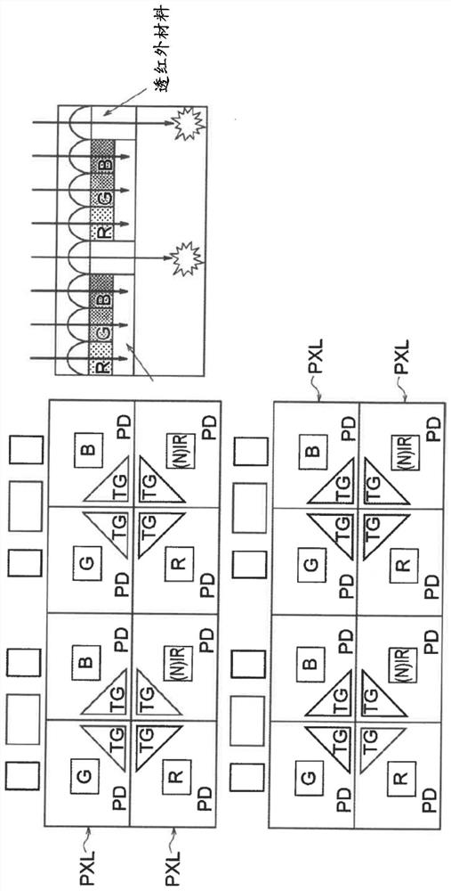
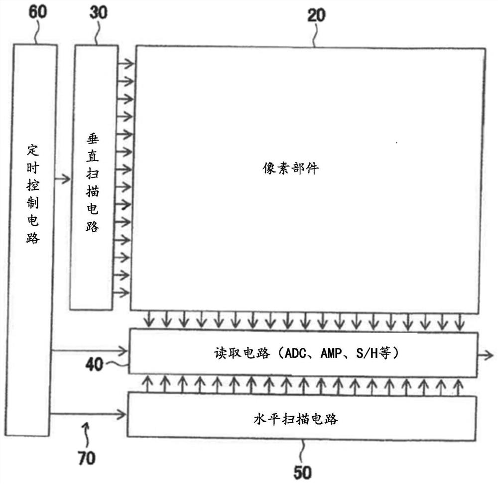
[0056] image 3 is a block diagram showing the configuration of the solid-state imaging device according to the first embodiment of the present invention. In this embodiment, the solid-state imaging device 10 is constituted by, for example, a CMOS image sensor.

[0057] Such as image 3 As shown, the solid-state imaging device 10 is mainly composed of a pixel unit 20 serving as an image capturing unit, a vertical scanning circuit (row scanning circuit) 30, a reading circuit (column reading circuit) 40, a horizontal scanning circuit (column scanning circuit) 50, and A timing control circuit 60 is configured. Among these components, for example, the vertical scanning circuit 30 , the reading circuit 40 , the horizontal scanning circuit 50 and the timing control circuit 60 constitute a reading section 70 for reading out pixel signals.

[0058] In the solid-state imaging device 10 according to the first embodiment, the pixel section 20 includes a unit pixel group including a pl...

no. 2 example

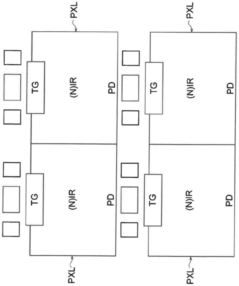
[0109] Figure 9 A reading operation in the second mode performed in the solid-state imaging device according to the second embodiment of the present invention is illustrated.

[0110] The second embodiment differs from the first embodiment in the following points. In the second embodiment, the reading section 70 can read from the Gb pixel PXL11 including the photodiode PD11 serving as the first green (Gb) photoelectric conversion section, including the photodiode PD12 serving as the blue (B) photoelectric conversion section. The B pixel PXL12, the R pixel PXL21 including the photodiode PD21 serving as a red (R) photoelectric conversion part, and the Gr pixel PXL22 including a photodiode PD22 serving as a second green (Gr) photoelectric conversion part simultaneously read (capture) visible light The color signal (RGB) in the infrared region and the infrared pixel signal (NIR) in the infrared region.

[0111] The solid-state imaging device 10A according to the second embodime...

no. 3 example

[0118] Figure 10 is a plan view showing a schematic arrangement of a configuration of a solid-state imaging device (CMOS image sensor) having a unit pixel group according to a third embodiment of the present invention. Figure 11 A reading operation in the first mode and a reading operation in the second mode performed in the solid-state imaging device according to the third embodiment of the present invention are illustrated.

[0119] The third embodiment differs from the first embodiment in the following points. The unit pixel groups 200B in the third embodiment are each formed as a unit RGBIR pixel group in which the filter of the PXL22 provided in the setting area AR22 is replaced by an infrared-dedicated pixel PXL22B including a pixel for receiving infrared light. Infrared (NIR) photoelectric conversion components.

[0120] In the first mode MOD1, the readout section 70 is set to output images from the G pixel PXL11 including the photodiode PD11 serving as the green ph...


PUM

PropertyMeasurementUnit
wavelengthaaaaaaaaaa

Abstract

An object of the present invention is to provide a solid-state imaging device that can capture visible light images such as RGB images and infrared images such as NIR images, and maintain high light-receiving sensitivity to infrared light, the object of the present invention It is also to provide a method of driving such a solid-state imaging device and an electronic device. The solid-state imaging device includes: a pixel section provided therein with a unit pixel group including a plurality of pixels for visible light performing photoelectric conversion capable of generating pixel signals; and a device for reading pixels from the pixel section. A reading part of a signal, wherein the plurality of pixels for visible light has light-receiving sensitivity to infrared light, and in an infrared reading mode, the reading part is arranged to convert the infrared light from the plurality of pixels for visible light of the pixel signal combined.

Description

[0001] Cross References to Related Applications [0002] This application is based on Japanese Patent Application No. 2017-230521 (filed on November 30, 2017) and Japanese Patent Application No. 2018-194303 (filed on October 15, 2018) and claims the priority rights thereof, and by way of reference The contents of which are incorporated herein in their entirety. technical field [0003] The present invention relates to a solid-state imaging device, a method for driving the solid-state imaging device, and electronic equipment. Background technique [0004] Realization of a solid-state imaging device (image sensor) including a photoelectric conversion element for detecting light and generating charge as a CMOS (Complementary Metal Oxide Semiconductor) image sensor is already in practical use. CMOS image sensors have been widely used as components of various electronic devices such as digital cameras, video recorders, surveillance video recorders, medical endoscopes, personal c...

Claims


Application Information

Patent Timeline
Patent Type & Authority Patents(China)
IPC IPC(8): H04N5/225H04N5/33H04N5/374H04N5/3745H04N5/378H01L27/146
CPCH04N5/33H01L27/14621H04N23/54H04N25/772H04N25/778H04N25/76H04N25/75
Inventor 田中俊介大高俊德阿久津贵弘
Owner 普里露尼库斯新加坡私人有限公司
Why Eureka
Try Eureka