Method for preparing circuit board and circuit board

A circuit board and area technology, applied in printed circuit manufacturing, printed circuits, printed circuit coatings, etc., can solve the problems of ink shedding, ink thickness, unevenness, light transmission on the surface of circuit boards, etc., to achieve uniform distribution of electrostatic fields, improve quality effect

Active Publication Date: 2020-10-16
NEW FOUNDER HLDG DEV LLC +1
View PDF4 Cites 0 Cited by
  • Summary
  • Abstract
  • Description
  • Claims
  • Application Information

AI Technical Summary

Problems solved by technology

[0005] The invention provides a method for preparing a circuit board and the circuit board, which are used to solve the problems of light transmission on the product surface of the existing circuit board, ink shedding and uneven thickness of the ink, etc.

Method used


Image

  • Method for preparing circuit board and circuit board
  • Method for preparing circuit board and circuit board
  • Method for preparing circuit board and circuit board

Examples


Embodiment Construction

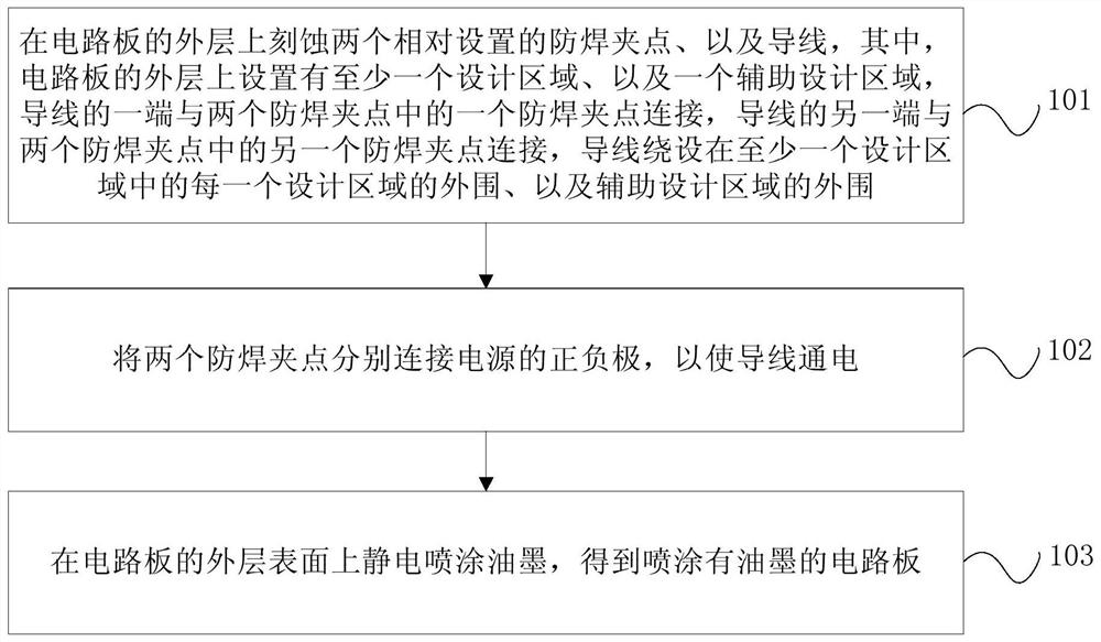
[0042] Reference will now be made in detail to the exemplary embodiments, examples of which are illustrated in the accompanying drawings. When the following description refers to the accompanying drawings, the same numerals in different drawings refer to the same or similar elements unless otherwise indicated. The implementations described in the following exemplary examples do not represent all implementations consistent with the present disclosure. Rather, they are merely examples of apparatuses and methods consistent with aspects of the present disclosure as recited in the appended claims.

[0043] At first the terms involved in the present invention are explained:

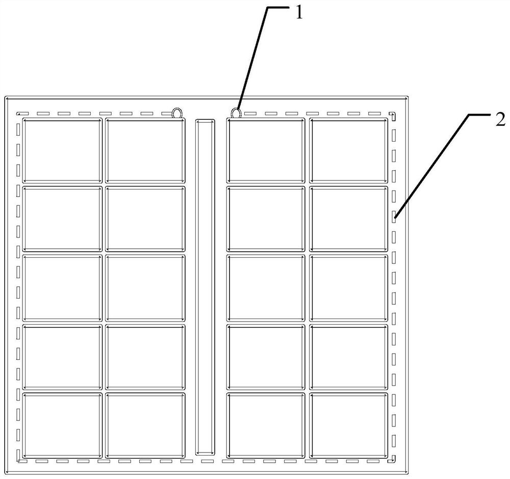
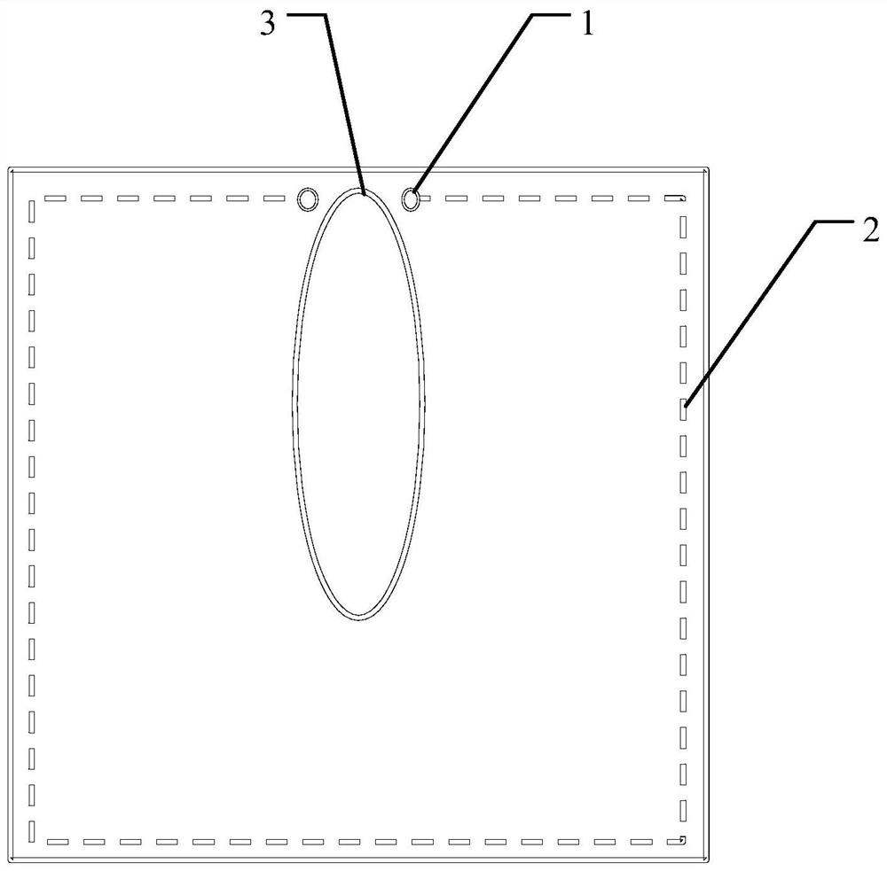
[0044] PCB: It is an important electronic component, a support for electronic components, and a carrier for electrical connections of electronic components.

[0045] The specific application scene of the present invention is: with the rapid development of electronic communication technology, the circuit board t...


PUM


Abstract

The present invention provides a preparation method of a circuit board and a circuit board. Two oppositely arranged anti-soldering clamp points and a wire are etched at the outer layer of the circuitboard, the outer layer of the circuit board is provided with at least one design region and an assistant design region, one end of the wire is connected with one of the two anti-soldering clamp points, the other end of the wire is connected with the other one of the anti-soldering clamp points, and the wire winds the periphery of each design region in the at least one design region and the periphery of the assistant design region; the two anti-soldering clamp points are respectively connected with the positive and negative poles of the power source to power on the wire; and the surface of theouter layer of the circuit board is subjected to electrostatic spraying with printing ink to obtain a circuit board sprayed with printing ink. In the preparation process of the circuit board, printingink charged particles are uniformly attached onto the surface of the outer layer of the circuit board so that the whole thickness of the printing ink layer of the surface of the circuit board is uniform and appropriate to improve the quality of the circuit board.

Description

technical field [0001] The invention relates to the technical field of circuit boards, in particular to a method for preparing a circuit board and the circuit board. Background technique [0002] With the rapid development of electronic communication technology, the process technology of printed circuit board (referred to as PCB) is also constantly developing. In the manufacturing process of the circuit board, the ink solder mask technology on the surface of the circuit board is one of the most important process technologies in the PCB product process. [0003] In the prior art, the anti-solder technology of ink on the surface of the circuit board adopts an electrostatic spraying process; in the prior art, two anti-solder pinch points are set on the outer layer of the circuit board, and then a wire is arranged on the outer layer of the circuit board, And the wire is arranged on the periphery of the outer layer of the entire circuit board, one end of the wire is connected to...

Claims


Application Information

Patent Timeline
Patent Type & Authority Patents(China)
IPC IPC(8): H05K3/28H05K3/00
CPCH05K3/0091H05K3/282H05K2203/0736H05K2203/1377
Inventor 车世民陈德福李晋峰叶万全王世威
Owner NEW FOUNDER HLDG DEV LLC
Why Eureka
Try Eureka