Lens three-dimensional contour measuring device and method based on current wave number scanning
A technology of three-dimensional profile and measuring device, which is applied in the direction of measuring device, optical device, machine/structural component testing, etc. It can solve the problems of slow image acquisition speed, complicated and expensive experimental device, and high environmental requirements, so as to avoid blur effect, Easy implementation and good device stability
- Summary
- Abstract
- Description
- Claims
- Application Information
AI Technical Summary
Problems solved by technology
Method used
Image

Examples
Embodiment 1
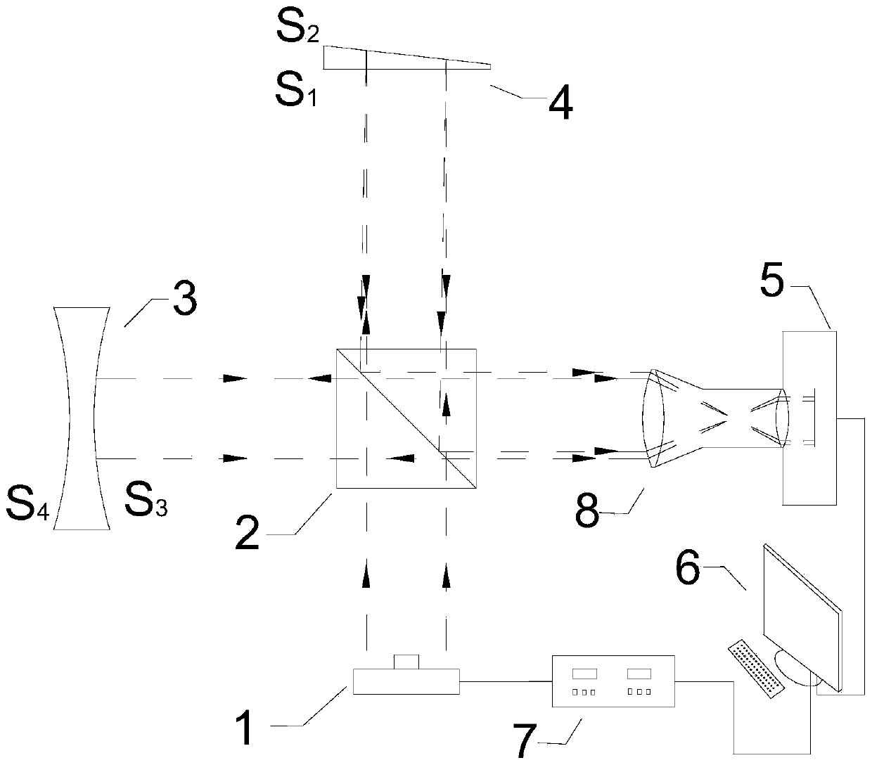
[0057] Such as Figure 1 to Figure 3 As shown, this embodiment discloses a lens three-dimensional profile measurement device based on current wavenumber scanning, the three-dimensional profile measurement device mainly includes a semiconductor laser 1 that emits relevant light, a beam splitting prism 2 that divides the relevant light into two parts, and an optical wedge 4. A CCD camera 5 for capturing the interference spectrum of reflected light, a computer 6 for processing image information, a laser controller 7 for adjusting the operating temperature and current of the semiconductor laser 1, and a bi-telecentric lens 8 for improving measurement accuracy.
[0058] Specifically, the semiconductor laser 1, the bi-telecentric lens 8, the optical wedge 4, and the lens under test 3 are sequentially arranged counterclockwise, and the beam splitting prism 2 is located at the center. The relevant light is emitted from the semiconductor laser 1, passes through the dichroic prism 2, an...
Embodiment 2
[0094] See attached Figure 1 to Figure 4 As shown, a kind of lens three-dimensional profile measurement device based on current wavenumber scanning described in the present embodiment is composed of semiconductor laser 1, beam splitting prism 2, lens, optical wedge 4, CCD camera 5, bi-telecentric lens 8, computer 6 and The laser controller consists of 7 components. Among them, the model of the semiconductor laser 1 is HL63603TG; the center thickness of the optical wedge 4 is 6 mm, and the inclination angle is 6'.
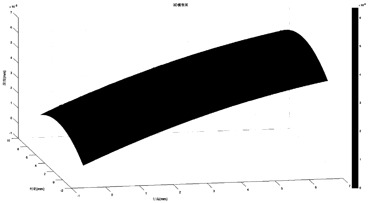
[0095] The measurement steps and principles of the present embodiment are as follows:
[0096] (1) Before the camera collects data, use the Tsai two-step method to calibrate the camera;
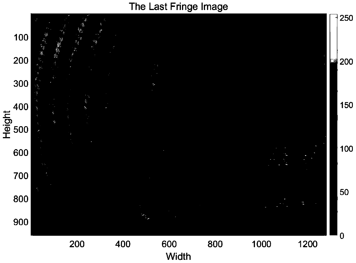
[0097] (2) computer 6 controls the exposure time of CCD camera 5, collection interval time and collection quantity; The correlation value of laser controller 7 is set;
[0098] (3) The laser controller 7 controls the operating current of the semiconductor laser 1 so that it emi...
PUM
 Abstract
Description
Claims
Application Information
 - R&D Engineer
- R&D Manager
- IP Professional
- Industry Leading Data Capabilities
- Powerful AI technology
- Patent DNA Extraction
Browse by: Latest US Patents, China's latest patents, Technical Efficacy Thesaurus, Application Domain, Technology Topic.
© 2024 PatSnap. All rights reserved.Legal|Privacy policy|Modern Slavery Act Transparency Statement|Sitemap