Display device, display panel and manufacturing method thereof

A technology for display panels and manufacturing methods, which is applied in semiconductor/solid-state device manufacturing, diodes, organic semiconductor devices, etc., can solve problems such as optical interference, and achieve the effect of ensuring clarity and solving optical interference

Active Publication Date: 2021-01-26
YUNGU GUAN TECH CO LTD
View PDF5 Cites 0 Cited by
  • Summary
  • Abstract
  • Description
  • Claims
  • Application Information

AI Technical Summary

Problems solved by technology

[0003] In order to solve the technical problem of optical interference caused by the graphic area in the prior art, the object of the present invention is to provide a display panel and a manufacturing method thereof, as well as a display device having the display panel

Method used


Image

  • Display device, display panel and manufacturing method thereof
  • Display device, display panel and manufacturing method thereof
  • Display device, display panel and manufacturing method thereof

Examples


Embodiment Construction

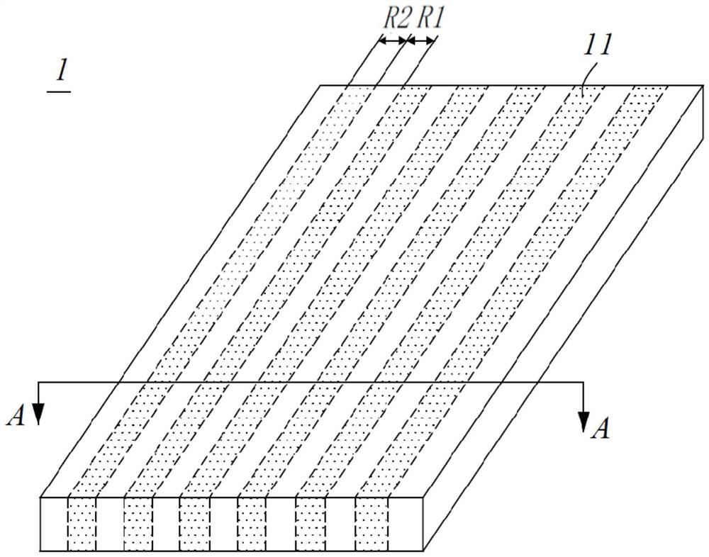
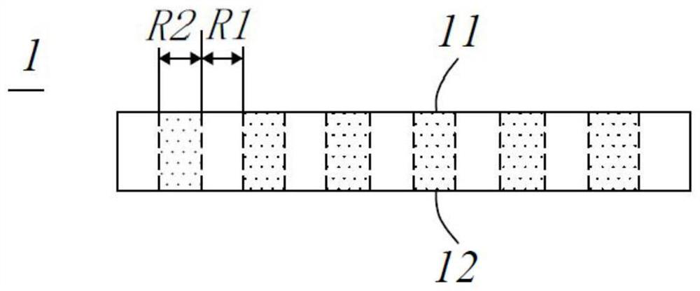
[0037] As described in the background, in the prior art, when a hidden camera component is arranged under a transparent PMOLED display panel, when light passes through the display panel, the electrode pattern area of ​​the display panel will cause optical interference, for example, when light passes through the display panel, due to the display The grating diffraction caused by the existence of the anode pattern and the cathode pattern of the panel makes it impossible for the camera component to achieve clear optical imaging.

[0038] Based on this, the present invention provides an electrode layer, a display panel having the electrode layer, and a display device, wherein the electrode layer cancels the graphic design in the prior art, but adopts a partially conductive monolithic film structure, so as to avoid the optical interference effect of graphic design in the prior art, and ensure clear imaging of the camera components.

[0039] Attached below Figures 1 to 8 A specifi...


PUM


Abstract

The invention discloses a display device, a display panel and a manufacturing method thereof. The display panel includes a light-emitting functional layer and two electrode layers, the electrode layer has a first surface and a second surface opposite to the first surface in the thickness direction, one of the electrode layers, the light-emitting function layer and another electrode layer are sequentially stacked and arranged in the thickness direction, and the first surface of each electrode layer is in contact with the light-emitting functional layer; each electrode layer includes a barrier area and an electrode region, the electrode region and the blocking region are cross-linked with each other as a whole, the material of the electrode region is a conductive modification of the material of the blocking region, the electrode region is in contact with the light-emitting functional layer and at least The first surface presents a conductor state. The invention cancels the physical conductive pattern of the cathode layer and the anode layer of the existing PMOLED, and solves the optical interference caused by the design of the conductive pattern in the prior art.

Description

technical field [0001] The invention relates to a display panel, a manufacturing method thereof, and a display device, belonging to the technical field of display. Background technique [0002] At present, in the PMOLED field, electrodes (such as cathodes and anodes) are usually a layer of conductive patterns protruding from the surface of the substrate. For the PMOLED structure with hidden camera components under the transparent display panel, when light passes through the display panel, the pattern area will cause Optical interference (such as interference and diffraction) makes it impossible for the camera components to achieve clear optical imaging. Contents of the invention [0003] In order to solve the technical problem of optical interference caused by the graphic area in the prior art, the purpose of the present invention is to provide a display panel, a manufacturing method thereof, and a display device having the display panel. [0004] In order to achieve one ...

Claims


Application Information

Patent Timeline
Patent Type & Authority Patents(China)
IPC IPC(8): H01L27/32H01L51/52H01L51/56
CPCH10K59/65H10K59/179H10K50/81H10K50/82H10K59/10H10K71/00H10K71/30H10K71/621H10K59/805H10K50/813H10K50/822H10K50/828H10K2102/101H10K2102/102H10K2102/103
Inventor 林立蔡世星楼均辉
Owner YUNGU GUAN TECH CO LTD
Why Eureka
Try Eureka