

Display
A display, thin film transistor technology, applied in the field of displays with a new test pad layout design, can solve problems such as limited space
- Summary
- Abstract
- Description
- Claims
- Application Information
AI Technical Summary
Problems solved by technology
Method used
Image

Examples
Embodiment 1
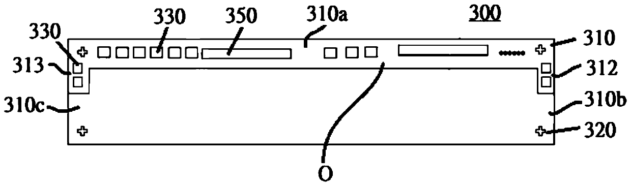
[0030] Accordingly, according to an embodiment 1 of the present invention, the present invention provides a display 300, see image 3 . image 3 It is a schematic diagram of arrangement of chip test pads of a display according to an embodiment of the present invention. like image 3 As shown, specifically, a display 300 according to an embodiment of the present invention includes: a thin film transistor (TFT) substrate 310; a color filter (CF) substrate 320, configured on the TFT substrate 310 and exposing the TFT substrate The first edge portion of the upper surface of the TFT substrate 310, wherein at least two corners of the CF substrate 320 each have a gap, the gap exposes the upper surface of the TFT substrate 310, forming at least two gap regions 312, 313 on the upper surface of the TFT substrate 310 ; and a plurality of chip test pads 330 are disposed on the first edge portion 310 a and the notch regions 312 , 313 .
[0031] continue to see image 3 , in Embodiment ...
Embodiment 2
[0039] According to an embodiment 2 of the present invention, the present invention provides a display 400, see Figure 4 . Figure 4 It is a schematic diagram of arrangement of chip test pads of a display according to another embodiment of the present invention. like Figure 4 As shown, specifically, a display 400 according to an embodiment of the present invention includes: a thin film transistor (TFT) substrate 410; a color filter (CF) substrate 420, configured on the TFT substrate 410 and exposing the TFT substrate The first edge portion of the upper surface of the TFT substrate 410, wherein at least two corners of the CF substrate 420 each have a gap, the gap exposes the upper surface of the TFT substrate 410, forming at least two gap regions 412, 413 On the upper surface of the TFT substrate 410 ; and a plurality of chip test pads 430 are disposed on the first edge portion 410 a and the notch areas 412 , 413 .
[0040] continue to see Figure 4 , in Embodiment 2 of t...
Embodiment 3
[0042] According to an embodiment 3 of the present invention, the present invention provides a display 500, see Figure 5 . Figure 5 It is a schematic diagram of arrangement of chip test pads of a display according to another embodiment of the present invention. like Figure 5 As shown, specifically, a display 500 according to an embodiment of the present invention includes: a thin film transistor (TFT) substrate 510; a color filter (CF) substrate 520, which is disposed on the TFT substrate 510 and exposes the TFT substrate The first edge portion of the upper surface of the TFT substrate 510, wherein at least two corners of the CF substrate 520 each have a gap, the gap exposes the upper surface of the TFT substrate 510, forming at least two gap regions 512, 513 on the upper surface of the TFT substrate 510; and a plurality of chip test pads 530 are disposed on the first edge portion 510a and the notch areas 512, 513.
[0043] continue to see Figure 5 , in Embodiment 3 of...
PUM
 Abstract
Description
Claims
Application Information