Pixel circuit and OLED display panel
A pixel circuit and circuit technology, applied in static indicators, instruments, etc., can solve the problems of short lifespan of OLED panels, and achieve the effect of alleviating electrochemical performance drift and improving short lifespan
- Summary
- Abstract
- Description
- Claims
- Application Information
AI Technical Summary
Problems solved by technology
Method used
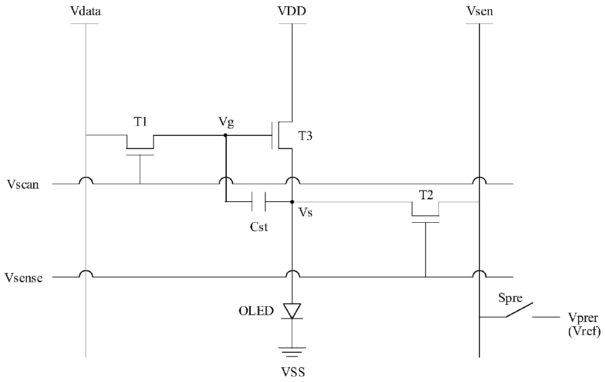
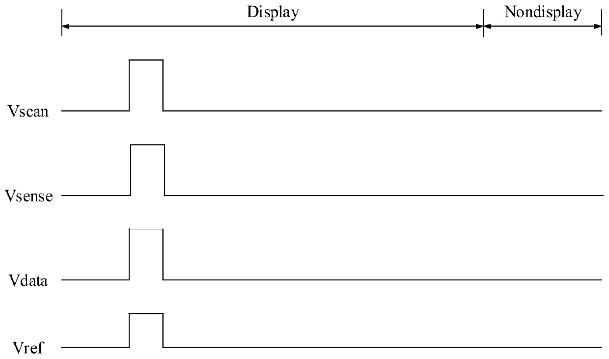
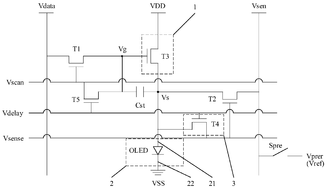
Image

Examples
Embodiment Construction
[0032] The technical solutions in the embodiments and / or examples of the present invention will be clearly and completely described below in conjunction with specific embodiments of the present invention. Obviously, the embodiments and / or examples described below are only part of the implementation of the present invention. schemes and / or examples, rather than all implementations and / or examples. Based on the implementations and / or examples in the present invention, all other implementations and / or examples obtained by those of ordinary skill in the art without creative efforts fall within the protection scope of the present invention.
[0033] The directional terms mentioned in the present invention, such as [top], [bottom], [left], [right], [front], [back], [inside], [outside], [side], etc., are only for reference The orientation of the attached schema. Therefore, the directional terms used are used to illustrate and understand the present invention, but not to limit the pr...
PUM
 Abstract
Description
Claims
Application Information
 - R&D Engineer
- R&D Manager
- IP Professional
- Industry Leading Data Capabilities
- Powerful AI technology
- Patent DNA Extraction
Browse by: Latest US Patents, China's latest patents, Technical Efficacy Thesaurus, Application Domain, Technology Topic.
© 2024 PatSnap. All rights reserved.Legal|Privacy policy|Modern Slavery Act Transparency Statement|Sitemap