Organic Light Emitting Components
A technology of organic light-emitting elements and light-emitting layers, which is applied in the fields of organic semiconductor devices, electrical components, light-emitting materials, etc., can solve problems such as difficulty in finding organic materials, and achieve the effects of improving performance, reducing element driving voltage, and improving luminous efficiency.
- Summary
- Abstract
- Description
- Claims
- Application Information
AI Technical Summary
Problems solved by technology
Method used
Image

Examples
Embodiment 1
[0053] Example 1 Fabrication of Fluorescent Organic Light-Emitting Elements
[0054] Before the substrate is loaded into the evaporation system for use, the substrate is cleaned with solvent and ultraviolet ozone for degreasing. Afterwards, the substrate is transferred to a vacuum deposition chamber where all layers are deposited on top of the substrate. Each layer is deposited by a heated evaporation boat in about 10 -6 The vacuum degree of Torr is deposited sequentially:
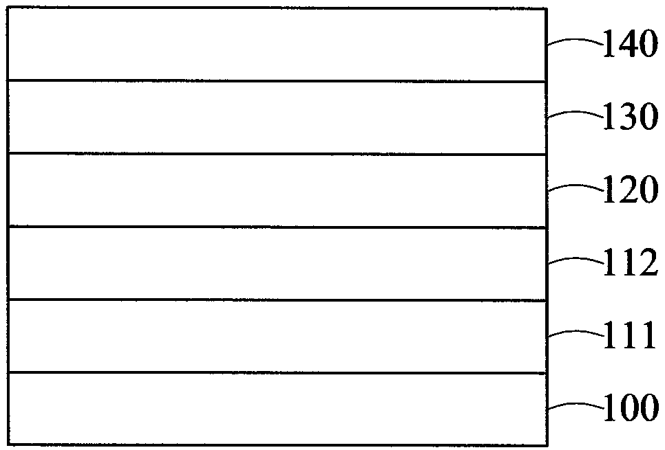
[0055] a) Indium tin oxide layer (ITO), thickness
[0056] b) first hole assisting layer, thickness HI;
[0057] c) Second hole assisting layer, thickness A compound of formula (Ia);
[0058] d) The third hole assisting layer, thickness HT2 compounds;
[0059] e) Luminescent layer, thickness Contains the main illuminant EPH and 4% by weight of the guest illuminant BD doped therein, (BD and EPH are the trade names of Taiwan Yulei Optoelectronics Technology Co., Ltd.);
[0060] f) Electron tr...
Embodiment 2
[0072] Example 2 Manufacture of phosphorescence-emitting organic light-emitting element
[0073] Before the substrate is loaded into the evaporation system for use, the substrate is cleaned with solvent and ultraviolet ozone for degreasing. Afterwards, the substrate is transferred to a vacuum deposition chamber where all layers are deposited on top of the substrate. Each layer is deposited by a heated evaporation boat in about 10 -6 The vacuum degree of Torr is deposited sequentially:
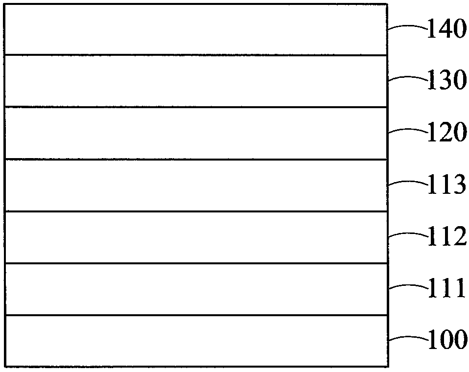
[0074] a) Indium tin oxide layer (ITO), thickness
[0075] b) first hole assisting layer, thickness HI;
[0076] c) Second hole assisting layer, thickness comprising a compound of formula (Ia) doped with 3% by weight of HI;
[0077] d) The third hole assisting layer, thickness HT2 compounds;
[0078] e) Luminescent layer, thickness Containing the main illuminant EPH and the guest illuminant PEG doped therein with 6% by weight of iridium metal complex (PEG and EPH are trade names ...
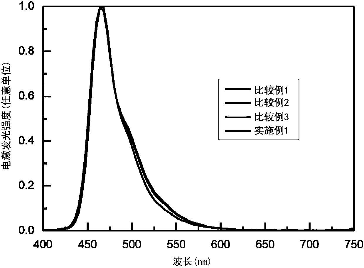
Embodiment 3 and 4
[0083] Examples 3 and 4 Manufacture of phosphorescence-emitting organic light-emitting elements
[0084] The organic light-emitting element of Example 3 was fabricated in the same manner as Example 2, with the difference that only the compound of formula (Ia) was used as the compound of the second hole assisting layer in Example 3.
[0085] The device structure of Example 3 can be represented as: ITO / HI / (Ia) / HT2 / PEG:EPH / Liq:ET / LiF / Al.
[0086] The manufacture of the organic light-emitting element in Example 4 is carried out in the same manner as in Example 2, with the difference that Example 4 does not have a third hole-assisting layer, and the thickness of the second hole-assisting layer is
PUM
 Abstract
Description
Claims
Application Information
 - R&D Engineer
- R&D Manager
- IP Professional
- Industry Leading Data Capabilities
- Powerful AI technology
- Patent DNA Extraction
Browse by: Latest US Patents, China's latest patents, Technical Efficacy Thesaurus, Application Domain, Technology Topic.
© 2024 PatSnap. All rights reserved.Legal|Privacy policy|Modern Slavery Act Transparency Statement|Sitemap