Display panel and manufacturing method thereof

A technology for a display panel and a manufacturing method, which is applied in the manufacture of semiconductor/solid-state devices, electrical components, and electrical solid-state devices, etc., can solve the problems of many manufacturing processes, high production costs, and complex structures of oxide film thin-film transistors, and can simplify the film Layer structure, reduction of processes and effects of reduction in number

Inactive Publication Date: 2019-08-02
SHENZHEN CHINA STAR OPTOELECTRONICS SEMICON DISPLAY TECH CO LTD
View PDF4 Cites 6 Cited by
  • Summary
  • Abstract
  • Description
  • Claims
  • Application Information

AI Technical Summary

Problems solved by technology

[0005] The embodiments of the present disclosure provide a display panel and a manufacturing method, which are used to solve the problems of the existing oxide film thin film transistors with complex structures, many manufacturing processes, and high production costs.

Method used


Image

  • Display panel and manufacturing method thereof
  • Display panel and manufacturing method thereof
  • Display panel and manufacturing method thereof

Examples


Embodiment 1

[0041] The disclosed embodiment provides a display panel, which is combined with Figure 1 to Figure 2 Describe in detail.

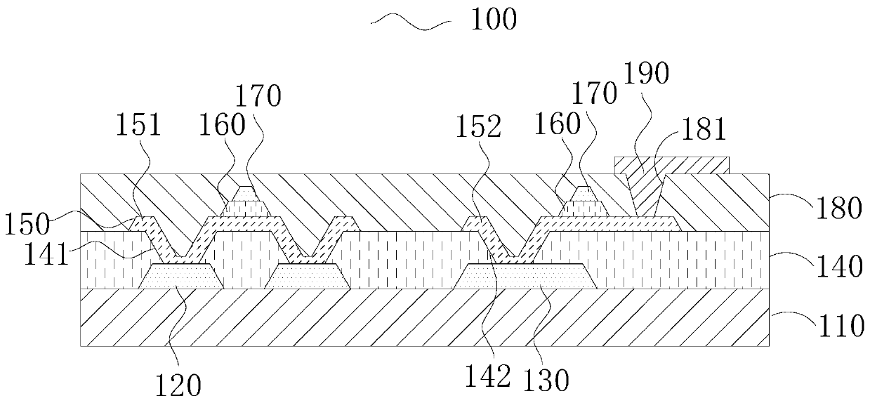
[0042] like figure 1 as shown, figure 1 A schematic cross-sectional structure diagram of the display panel 100 provided by an embodiment of the present disclosure. The display panel 100 includes a substrate 110 , source and drain electrodes 120 , a light shielding layer 130 , a dielectric layer 140 and an oxide semiconductor layer 150 .

[0043] In this embodiment, the source-drain electrodes 120 are disposed on the substrate 110, the light-shielding layer 130 is disposed on the substrate 110, and the light-shielding layer 130 and the source-drain electrodes 120 are disposed on the same layer. . The dielectric layer 140 is disposed on the substrate 110 and covers the light shielding layer 130 and the source-drain electrodes 120, the dielectric layer 140 is provided with a first via hole 141 and a second via hole 142, the The first via hole 141 and t...

Embodiment 2

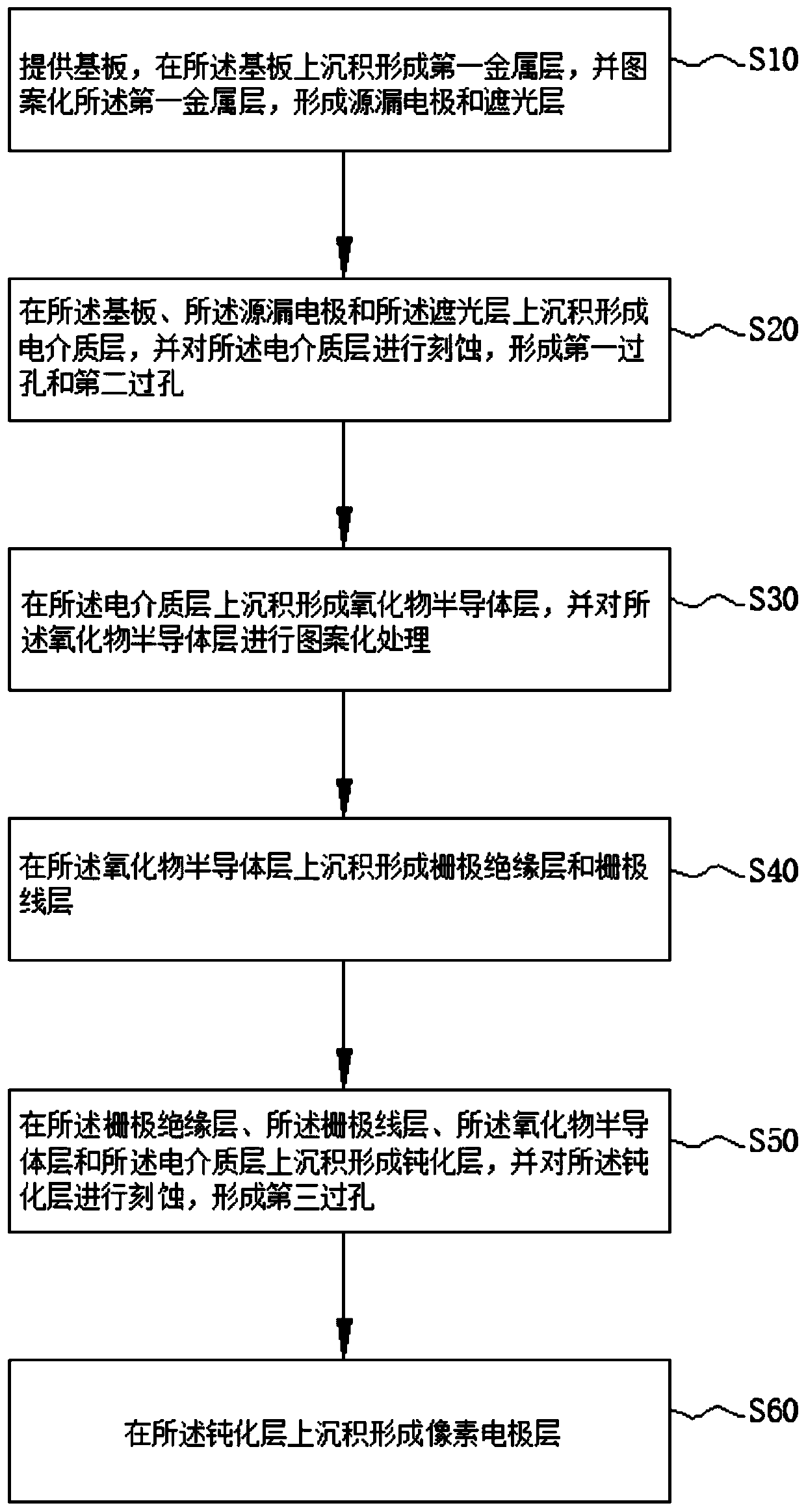
[0062] The disclosed embodiment also provides a manufacturing method of the display panel 200, which is combined with Figure 3 to Figure 9 Describe in detail. Described preparation method comprises:

[0063] Step S10, such as Figure 4 As shown, a substrate 210 is provided, a first metal layer is deposited and formed on the substrate 210 , and the first metal layer is patterned to form a source-drain electrode 220 and a light-shielding layer 230 .

[0064] In this embodiment, the first metal layer is a laminated structure of molybdenum and copper or a laminated structure of aluminum and molybdenum.

[0065] Step S20: if Figure 5 As shown, a dielectric layer 240 is deposited and formed on the substrate 210, the source-drain electrodes 220 and the light-shielding layer 230, and the dielectric layer 240 is etched to form a first via hole 241 and a second via hole 242.

[0066] In this embodiment, the material of the dielectric layer 240 includes SiOx, and in some embodimen...


PUM


Abstract

The invention provides a display panel and a manufacturing method thereof. The display panel comprises a substrate, a source / drain electrode, a light shielding layer, a dielectric layer and an oxide semiconductor layer. The oxide semiconductor layer is arranged on the dielectric layer and is connected with the source / drain electrode and the light shielding layer through a first via hole and a second via hole. The source / drain electrode and the light shielding layer are arranged on the same layer of the substrate, the source / drain electrode and the light shielding layer are simultaneously formed by etching the first metal layer and the dielectric layer is arranged on the substrate and covers the light shielding layer and the source / drain electrode layer so that that dielectric layer is enabled to have the function of the isolation layer, thereby reducing the number of the film layers of the display panel, simplifying the film layer structure of the display panel, simultaneously reducingthe processes required for production and the use number of the mask plate, improving the production efficiency and reducing the production cost.

Description

technical field [0001] The present invention relates to the technical field of display device manufacturing, in particular to a display panel and a manufacturing method. Background technique [0002] As an electronic information industry with development potential, the display device industry has developed rapidly in recent years. Its mainstream organic light emitting diode (Organic Light Emitting Diode, OLED) display device industry has become one of the pillar industries in the electronic information industry. A thin film transistor (Thin Film Transistor, TFT) is a core device of a flat panel display, and in an OLED display device, a TFT is usually used as an address switching device. Hydrogenated amorphous silicon (a-Si:H) TFT is the most widely used TFT technology, but limited by its low carrier mobility, this technology cannot meet the high-definition image quality requirements of next-generation OLED display devices. TFT plays a vital role in OLED display pixel circu...

Claims


Application Information

Patent Timeline
Patent Type & Authority Applications(China)
IPC IPC(8): H01L27/12H01L21/77H01L27/32
CPCH01L27/1225H01L27/1259H10K59/1213H01L29/66969H01L29/78633H01L29/7869H01L21/02565H01L27/127
Inventor 卢马才
Owner SHENZHEN CHINA STAR OPTOELECTRONICS SEMICON DISPLAY TECH CO LTD
Why Eureka
Try Eureka