
Organic light-emitting diode device and manufacturing method thereof

A technology of light-emitting diodes and manufacturing methods, which is applied in semiconductor/solid-state device manufacturing, electric solid-state devices, semiconductor devices, etc., and can solve problems such as device light leakage

Active Publication Date: 2019-08-02
SHENZHEN CHINA STAR OPTOELECTRONICS SEMICON DISPLAY TECH CO LTD
View PDF7 Cites 5 Cited by
  • Summary
  • Abstract
  • Description
  • Claims
  • Application Information

AI Technical Summary

Problems solved by technology

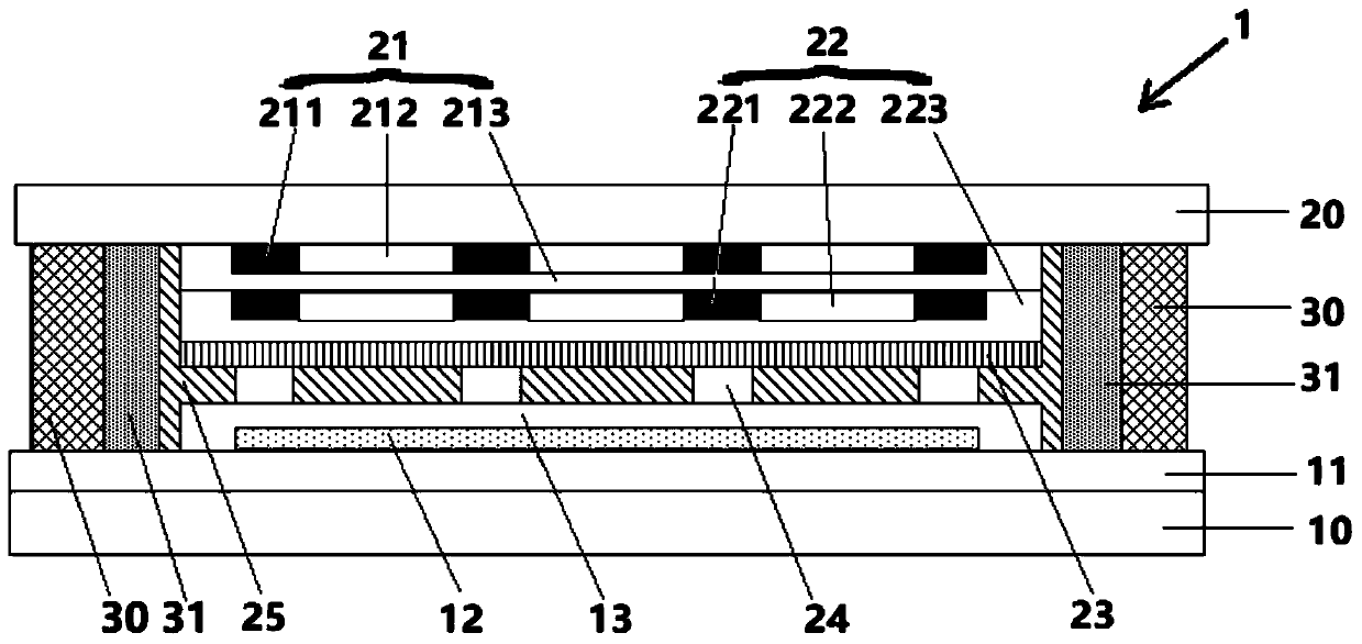
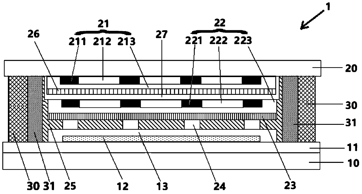
[0005] The object of the present invention is to provide an organic light emitting diode device and its manufacturing method, which can solve the problem of device light leakage caused by the thickness of the cell by reducing the cell distance between the glass substrate and the glass cover and setting an optical isolation layer to block light. question

Method used


Image

  • Organic light-emitting diode device and manufacturing method thereof
  • Organic light-emitting diode device and manufacturing method thereof
  • Organic light-emitting diode device and manufacturing method thereof

Examples


Embodiment Construction

[0040] In the present invention, unless otherwise clearly specified and limited, a first feature being "on" or "under" a second feature may include direct contact between the first and second features, and may also include the first and second features Not in direct contact but through another characteristic contact between them. Moreover, "above", "above" and "above" the first feature on the second feature include that the first feature is directly above and obliquely above the second feature, or simply means that the first feature is horizontally higher than the second feature. "Below", "beneath" and "under" the first feature to the second feature include that the first feature is directly below and obliquely below the second feature, or simply means that the first feature has a lower level than the second feature.

[0041] In the present invention, the same or corresponding components are represented by the same reference numerals regardless of the figure number, and throug...


PUM

PropertyMeasurementUnit
Thicknessaaaaaaaaaa
Thicknessaaaaaaaaaa
Thicknessaaaaaaaaaa

Abstract

The invention provides an organic light-emitting diode device and a manufacturing method thereof. The organic light-emitting diode device includes a glass substrate, a glass cover plate and a sealingglue layer, wherein an upper surface of the glass substrate sequentially includes an array substrate layer, an electroluminescence layer and a first film packaging layer, a lower surface of the glasscover plate sequentially includes a colorful filter, a quantum light emitting layer, an optical modulation layer and an optical isolation layer, and the optical isolation layer and a black light blocking layer of the colorful filter are oppositely arranged and are used for blocking the light emitted by the electroluminescence layer from leaking. The manufacturing method of the organic light-emitting diode device comprises steps of making the glass substrate, making the glass cover plate and packaging parts into a box. The organic light-emitting diode device is advantaged in that through reducing the box distance between the glass substrate and the glass cover plate and setting the optical isolation layer for light blocking, a problem of device light leakage caused by box thickness is solved.

Description

technical field [0001] The invention relates to the display field, in particular to an organic light emitting diode device and a manufacturing method thereof. Background technique [0002] An organic light emitting diode device (Organic Light Emitting Diode, OLED) is also called an organic electroluminescent display or an organic light emitting semiconductor. Because of its characteristics such as self-illumination, infinitely high contrast, wide viewing angle, low power consumption, extremely fast response speed, and flexible display, it has been regarded as a new generation of display technology since its discovery. [0003] QD-OLED takes into account the brightness of quantum dots, OLED's independent light emission and ultra-thin design. The industry is currently in the research and development stage, and its application in the display terminal market in the future may have a chance to emerge. QD-OLED is more like a combination of quantum dots and OLED. Using blue OLED a...

Claims


Application Information

Patent Timeline
IPC IPC(8): H01L51/50H01L51/52H01L51/56
CPCH10K50/13H10K50/84H10K71/00
Inventor 魏锋李金川
Owner SHENZHEN CHINA STAR OPTOELECTRONICS SEMICON DISPLAY TECH CO LTD
Learn More