Semiconductor structure and forming method thereof

A technology of semiconductor and stacked structure, which is applied in the direction of semiconductor devices, electric solid devices, electrical components, etc., can solve the problems of reduced bandgap width, memory performance degradation, and increased electron tunneling probability, so as to avoid the reduction of bandgap width and improve The effect of maintaining properties

Active Publication Date: 2019-08-09
YANGTZE MEMORY TECH CO LTD
View PDF5 Cites 6 Cited by
  • Summary
  • Abstract
  • Description
  • Claims
  • Application Information

AI Technical Summary

Problems solved by technology

However, in the actual process, due to the high N content in SiN of the electron trapping layer, the N element in the high N layer will diffuse to the low N region during the high temperature annealing process, so that the N element is doped into the barrier layer and the tunneling layer. The reduction of the forbidden band width increases the probability of electron tunneling, which reduces the retention characteristics of the device and the performance of the memory.
[0006] Therefore, the performance of the existing memory needs to be further improved

Method used


Image

  • Semiconductor structure and forming method thereof
  • Semiconductor structure and forming method thereof
  • Semiconductor structure and forming method thereof

Examples


Embodiment Construction

[0027] Specific implementations of the semiconductor structure and its forming method provided by the present invention will be described in detail below in conjunction with the accompanying drawings.

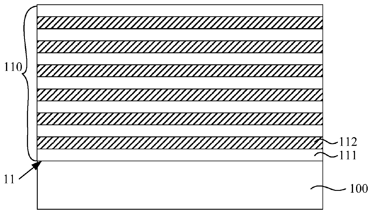
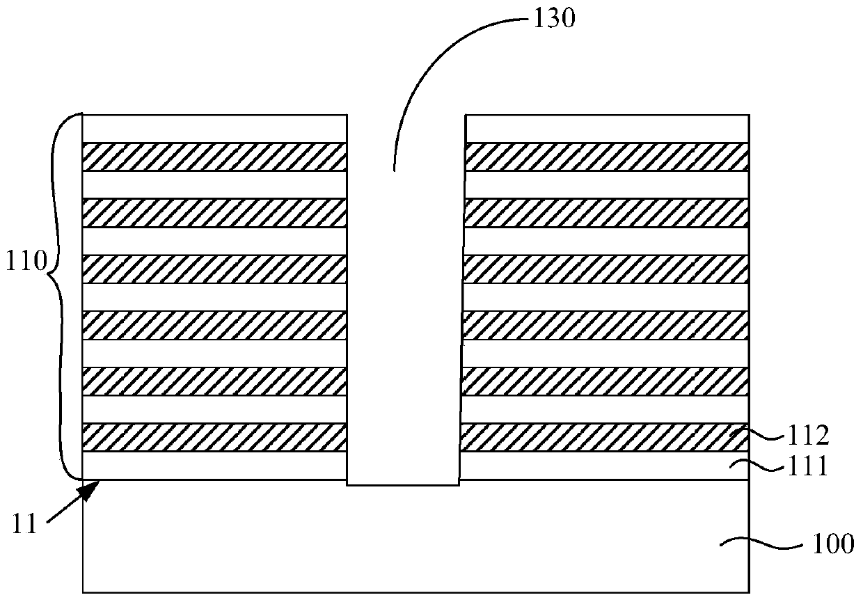
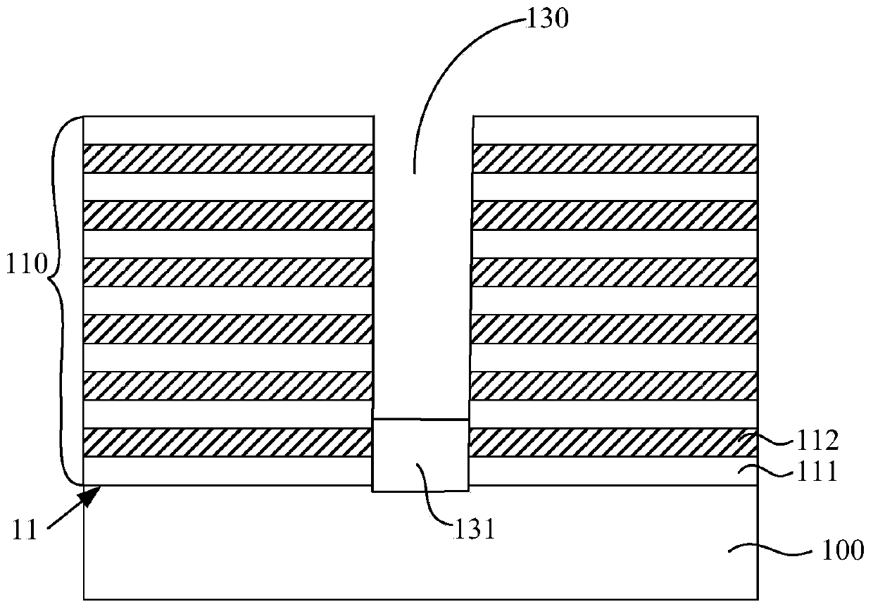
[0028] Please refer to Figure 1 to Figure 7 , is a structural schematic diagram of the formation process of the semiconductor structure according to a specific embodiment of the present invention. The semiconductor structure may be a memory or an intermediate product structure in the process of forming a memory.

[0029] Please refer to figure 1 A substrate 100 is provided, the substrate 100 has a first surface 11 , and a stack structure 110 is formed on the first surface 11 of the substrate 100 .

[0030] The substrate 100 can be a single crystal silicon substrate, a Ge substrate, a SiGe substrate, SOI or GOI, etc.; according to the actual requirements of the device, a suitable semiconductor material can be selected as the substrate 100, which is not limited here. In this...


PUM


Abstract

The invention relates to a semiconductor structure and a forming method thereof. The semiconductor structure comprises a substrate, wherein a stacked structure is formed on the surface of the substrate; a channel hole penetrating through the stacked structure to the surface of the substrate; a functional sidewall covering the sidewall of the channel hole and including an electron barrier layer, anelectron capturing layer and a tunneling layer which are successively stacked from the sidewall of the channel hole to the inside of the channel hole; and a diffusion barrier layer between the electron barrier layer and the electron capturing layer and/or between the electron capturing layer and the tunneling layer. The semiconductor structure has high retention characteristics.

Description

technical field [0001] The invention relates to the technical field of semiconductors, in particular to a semiconductor structure and a forming method thereof. Background technique [0002] In recent years, the development of flash memory (Flash Memory) is particularly rapid. The main feature of flash memory is that it can keep stored information for a long time without power on, and has the advantages of high integration, fast access speed, easy erasing and rewriting, etc. Has been widely used. In order to further increase the bit density (Bit Density) of the flash memory while reducing the bit cost (Bit Cost), three-dimensional flash memory (3D NAND) technology has been developed rapidly. [0003] A 3D NAND memory includes a storage stack structure and a channel structure running through the storage stack structure. The channel structure includes a channel hole penetrating through the memory stack structure, a functional layer covering sidewalls of the channel hole, and...

Claims


Application Information

Patent Timeline
Patent Type & Authority Applications(China)
IPC IPC(8): H01L27/1157H01L27/11582H01L29/792
CPCH01L29/7926H10B43/35H10B43/27
Inventor 王启光
Owner YANGTZE MEMORY TECH CO LTD
Why Eureka
Try Eureka