Display panel and display device

A display panel and substrate technology, applied in optics, instruments, character and pattern recognition, etc., can solve the problems affecting the imaging quality of optical fingerprint recognition sensors, the fingerprint module occupies a certain space, and the manufacturing process is difficult, so as to avoid interference, Solve the effect of backlight uniformity, cost and module thickness optimization

Inactive Publication Date: 2019-08-20
WUHAN CHINA STAR OPTOELECTRONICS TECH CO LTD
View PDF12 Cites 14 Cited by
  • Summary
  • Abstract
  • Description
  • Claims
  • Application Information

AI Technical Summary

Problems solved by technology

[0003] Currently, the under-display fingerprint recognition sensors on the market use silicon as the substrate, which is costly and difficult to manufacture, and is separated from the display screen, and the fingerprint module takes up a certain amount of space.
[0004] In addition, the side-light light-emitting diode (LED) backlight mainly used in the current liquid crystal display panel on the market, the light provided by the backlight system is not uniform, and the utilization rate of the light source is low, resulting in brighter fingerprint images near the light-emitting diodes, and brighter fingerprints near the light-emitting diodes. The fingerprint image in a distant place is relatively dark, which affects the imaging quality of the optical fingerprint recognition sensor

Method used


Image

  • Display panel and display device
  • Display panel and display device
  • Display panel and display device

Examples


Embodiment Construction

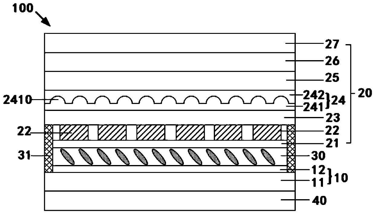
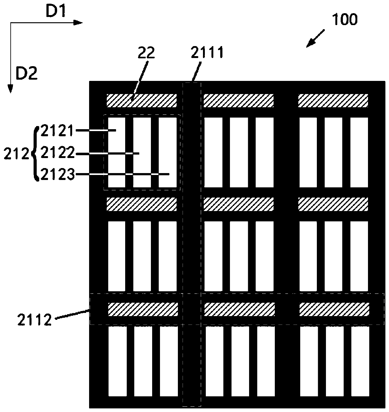
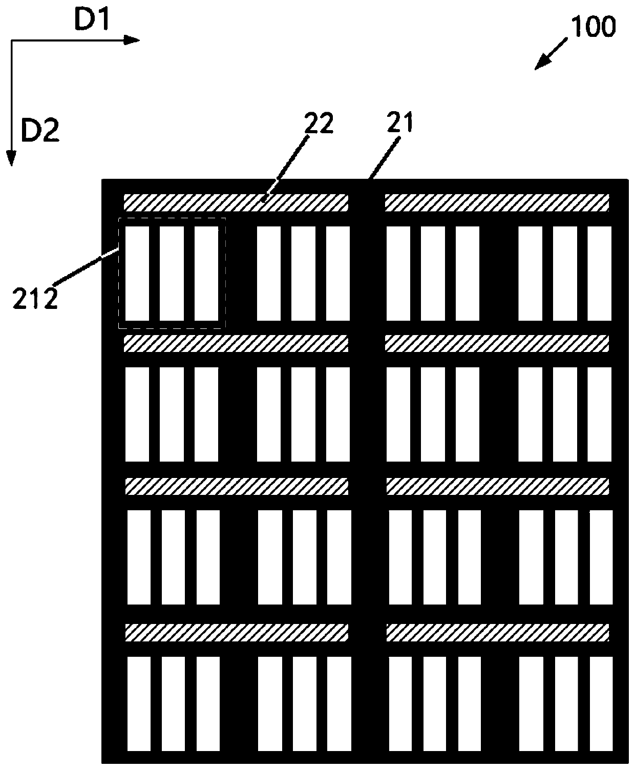
[0037] The following description of various embodiments is made with reference to the accompanying drawings to illustrate specific embodiments in which the invention may be practiced. The directional terms mentioned in the present invention, such as up, down, front, back, left, right, inside, outside, side, etc., are only directions referring to the drawings. The component names mentioned in the present invention, such as first, second, etc., are only used to distinguish different components, which can be better expressed. In the figures, structurally similar elements are denoted by the same reference numerals.

[0038] Embodiments of the present invention will be described in detail herein with reference to the accompanying drawings. This invention may be embodied in many different forms and should not be construed as only the specific embodiments set forth herein. These embodiments are provided to explain the practical application of the invention, so that others skilled i...


PUM


Abstract

The invention relates to a display panel and a display device. The display panel comprises a first substrate, a second substrate and a liquid crystal layer filled between the first substrate and the second substrate; the second substrate comprises a pixel layer provided with a plurality of pixel units, and at least one fingerprint identification unit which is arranged in the second substrate and located at a gap of the pixel units. The display device comprises the display panel. The fingerprint identification unit is manufactured on a color film substrate of the display panel, so that the display function / touch control function / fingerprint identification function is integrated, and the cost and the thickness of the module are more optimized; due to the arrangement of a concentration layer,interference of light rays can be avoided, and interference between adjacent pixel units is reduced. Furthermore, the uniformity of light rays can be improved by adopting a surface light source, so that the imaging quality of the fingerprint identification unit is improved.

Description

technical field [0001] The present invention relates to the field of display technology, in particular to a display panel and a display device. Background technique [0002] In existing display devices such as smart phones, the fingerprint identification sensor is usually placed at the position of the menu key (home key). With the advent of the full screen, the borders around the display screen are getting narrower and the home button is cancelled. Placing the fingerprint recognition sensor on the back or side of the mobile phone has become an intermediate transition solution. Placing it under the display screen or in the screen will be a major development of fingerprint recognition. trend. [0003] Currently, the under-display fingerprint recognition sensors on the market use silicon as the substrate, which is costly and difficult to manufacture, and is separated from the display screen, and the fingerprint module takes up a certain amount of space. [0004] In addition, ...

Claims


Application Information

Patent Timeline
Patent Type & Authority Applications(China)
IPC IPC(8): G02F1/1333G02F1/1335G02F1/13357G06K9/00
CPCG02F1/13338G02F1/133526G02F1/133611G06V40/1318G02F1/13312G02F1/133512G02F1/133514
Inventor 胡丽
Owner WUHAN CHINA STAR OPTOELECTRONICS TECH CO LTD
Why Eureka
Try Eureka