Calibration system and method for improving accuracy of chip internal reference voltage value

A technology of reference voltage and voltage value, applied in the field of electronics, can solve problems such as affecting chip calibration accuracy and poor contact, and achieve the effect of improving calibration efficiency, improving calibration accuracy and wide application range

Active Publication Date: 2021-06-18
CRM ICBG (WUXI) CO LTD
View PDF0 Cites 0 Cited by
  • Summary
  • Abstract
  • Description
  • Claims
  • Application Information

AI Technical Summary

Problems solved by technology

When the chip to be tested falls from the material tube of the semi-automatic programming machine, it will be caught by the golden finger of the semi-automatic programming machine, so that the chip to be tested is connected to the programmer through the golden finger, and because the gold in the semi-automatic programming machine The mechanical structure of the finger, when the gold finger grabs the chip to be tested, sometimes it will have poor contact, that is, there is a certain contact resistance, and the existence of contact resistance will affect the calibration accuracy of the chip

Method used


Image

  • Calibration system and method for improving accuracy of chip internal reference voltage value
  • Calibration system and method for improving accuracy of chip internal reference voltage value
  • Calibration system and method for improving accuracy of chip internal reference voltage value

Examples


Embodiment Construction

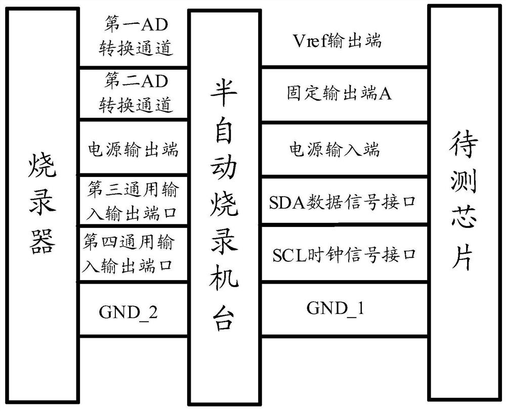
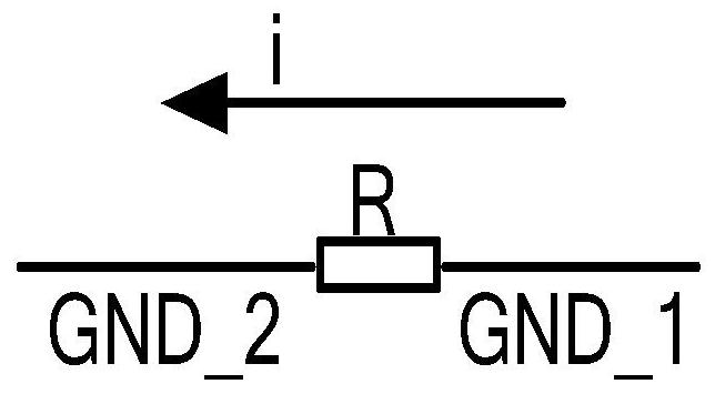
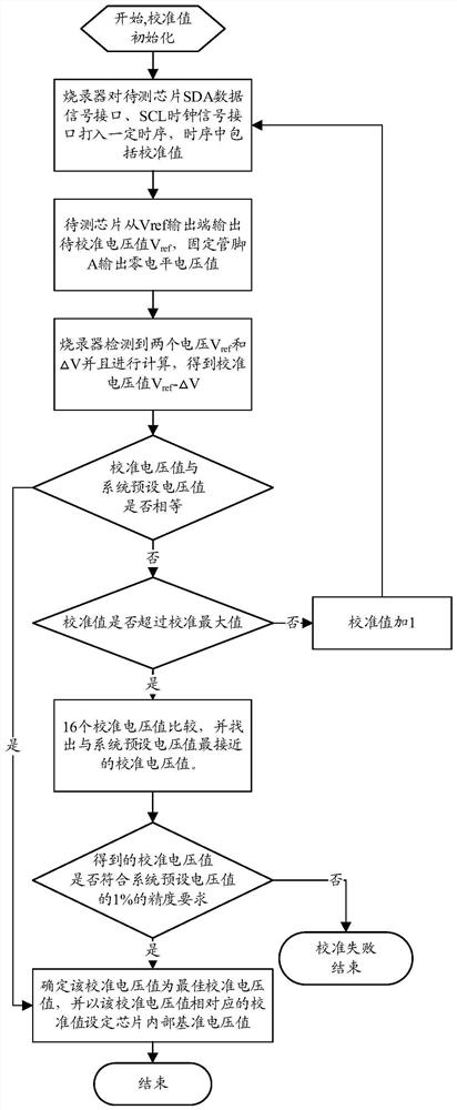
[0031] Before describing the embodiments according to the present invention in detail, it should be noted that the embodiments relate to a combination of a calibration system and a method for improving the accuracy of a reference voltage value inside a chip. The described circuit structure and each module unit are represented by conventional symbols at appropriate positions in the drawings, and only the details relevant to the understanding of the embodiments of the present invention are shown, so as not to disturb those skilled in the art who benefit from the present invention. The disclosure is obscured by details that would be apparent to one of ordinary skill.

[0032] Hereinafter, relational terms such as first and second are used merely to distinguish one entity or action from another without necessarily requiring or implying any actual such relationship or order between such entities or actions . The terms "comprising", "comprising" or any other variant are intended to...


PUM


Abstract

The invention relates to a calibration system and method for improving the accuracy of the internal reference voltage value of a chip, wherein the method includes that the burner first makes the chip to be tested enter the calibration process, and secondly, the burner cooperates with a semi-automatic burner to detect the The voltage value to be calibrated of the chip to be tested and the voltage difference between the two ends of the contact resistance, and the subtraction of the voltage value to be calibrated of the chip to be tested and the voltage difference between the two ends of the contact resistance is performed to obtain the current calibration value corresponding to the The calibration voltage value of the chip to be tested, and finally the programmer completes the calibration of the internal reference voltage value of the chip to be tested according to the judgment result of whether there is an optimal calibration voltage value.

Description

technical field [0001] The invention relates to the field of electronics, in particular to the field of testing, in particular to a calibration system and method for improving the accuracy of a chip internal reference voltage value. Background technique [0002] There is often a certain deviation between the chip and the system preset voltage value, so it needs to be calibrated. In this process, the programmer is used in conjunction with the semi-automatic programming machine, so that the programmer and the semi-automatic programming At the same time, the burner is connected to the chip through a gold finger. The gold finger is a large number of golden conductive contacts inside the semi-automatic burner. Because the surface is gold-plated and the conductive contacts are arranged like fingers, it is called "" Goldfinger". When the chip to be tested falls from the material tube of the semi-automatic programming machine, it will be caught by the golden finger of the semi-auto...

Claims


Application Information

Patent Timeline
Patent Type & Authority Patents(China)
IPC IPC(8): G01R19/25
CPCG01R19/2506
Inventor 孙红新顾晓红赵海
Owner CRM ICBG (WUXI) CO LTD
Why Eureka
Try Eureka