

Chip packaging method
A packaging method and chip technology, which can be used in the manufacture of electrical components, electrical solid devices, semiconductors/solid devices, etc., and can solve problems such as low chip efficiency
- Summary
- Abstract
- Description
- Claims
- Application Information
AI Technical Summary
Problems solved by technology
Method used
Image



Examples
Embodiment Construction
[0023] As mentioned in the background art, the efficiency of embedding micro light-emitting diodes using existing packaging methods is low.
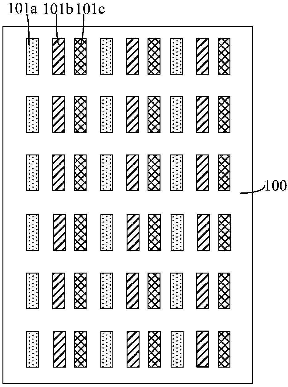
[0024] figure 1 It is a structural schematic diagram of a chip package structure with different sizes.
[0025] Please refer to figure 1 , providing the substrate 100, the substrate 100 has a plurality of mutually separated first openings (not shown in the figure), second openings (not shown in the figures) and third openings (not shown in the figures); Utilize manipulator (not shown in the figure), embed red chip 101a in the first opening, embed green chip 101b in the second opening, embed blue chip 101c in the 3rd opening, and described red chip 101a, green chip 101b and blue chip 101c are different in size from each other.
[0026] In the above method, in order to realize the embedding of the red chip 101a, the green chip 101b and the blue chip 101c, the red chip 101a, the green chip 101b and the blue chip 101c are respectively emb...
PUM
 Abstract
Description
Claims
Application Information