Thin Film Transistor Substrate and Method of Fabricating the Same

a technology of thin film transistors and substrates, applied in the direction of instruments, semiconductor devices, electrical equipment, etc., can solve the problems of increasing process costs and process tim

Active Publication Date: 2013-04-11
LG DISPLAY CO LTD
View PDF1 Cites 35 Cited by
  • Summary
  • Abstract
  • Description
  • Claims
  • Application Information

AI Technical Summary

Benefits of technology

[0022]During the lift-off process, a stripper may permeate the space between the first photoresist pattern and the third passivation film and thus separate the first photoresist pattern and the second transparent electrode layer formed thereon from the third passivation film.

Problems solved by technology

The method of fabricating the FFS mode thin film transistor substrate requires at least seven mask processes, as described above, and may thus cause increase in process costs and process time.

Method used


Image

  • Thin Film Transistor Substrate and Method of Fabricating the Same
  • Thin Film Transistor Substrate and Method of Fabricating the Same
  • Thin Film Transistor Substrate and Method of Fabricating the Same

Examples


Embodiment Construction

[0039]Reference will now be made in detail to the preferred embodiments of the present invention, examples of which are illustrated in the accompanying drawings. Configuration of the present invention and function thereby will be given through detailed description below. Wherever possible, the same reference numbers will be used throughout the drawings to refer to the same or like parts. In the following description of the present invention, a detailed description of known functions and configurations incorporated herein will be omitted when it may make the subject matter of the present invention rather unclear.

[0040]Hereinafter, a preferred embodiment of the present invention will be described with reference to FIGS. 1 to 8F.

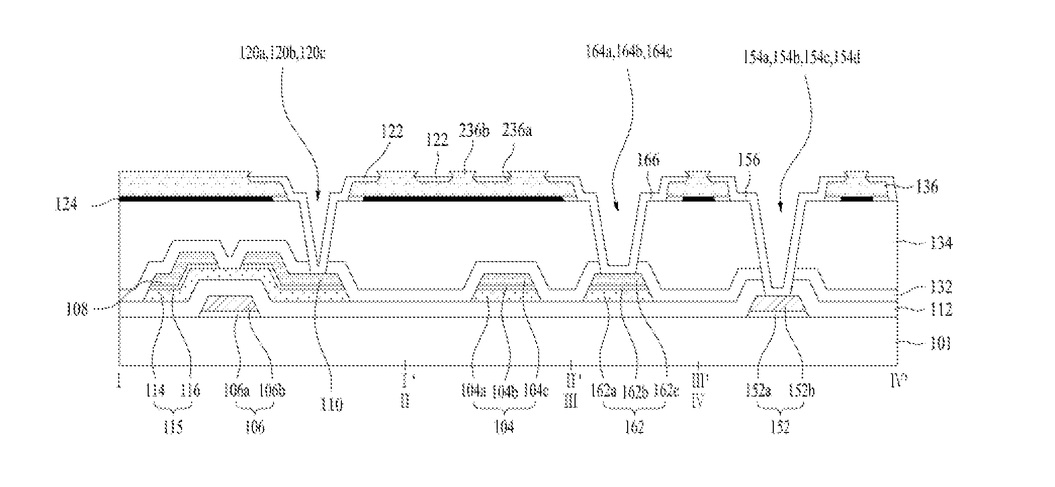
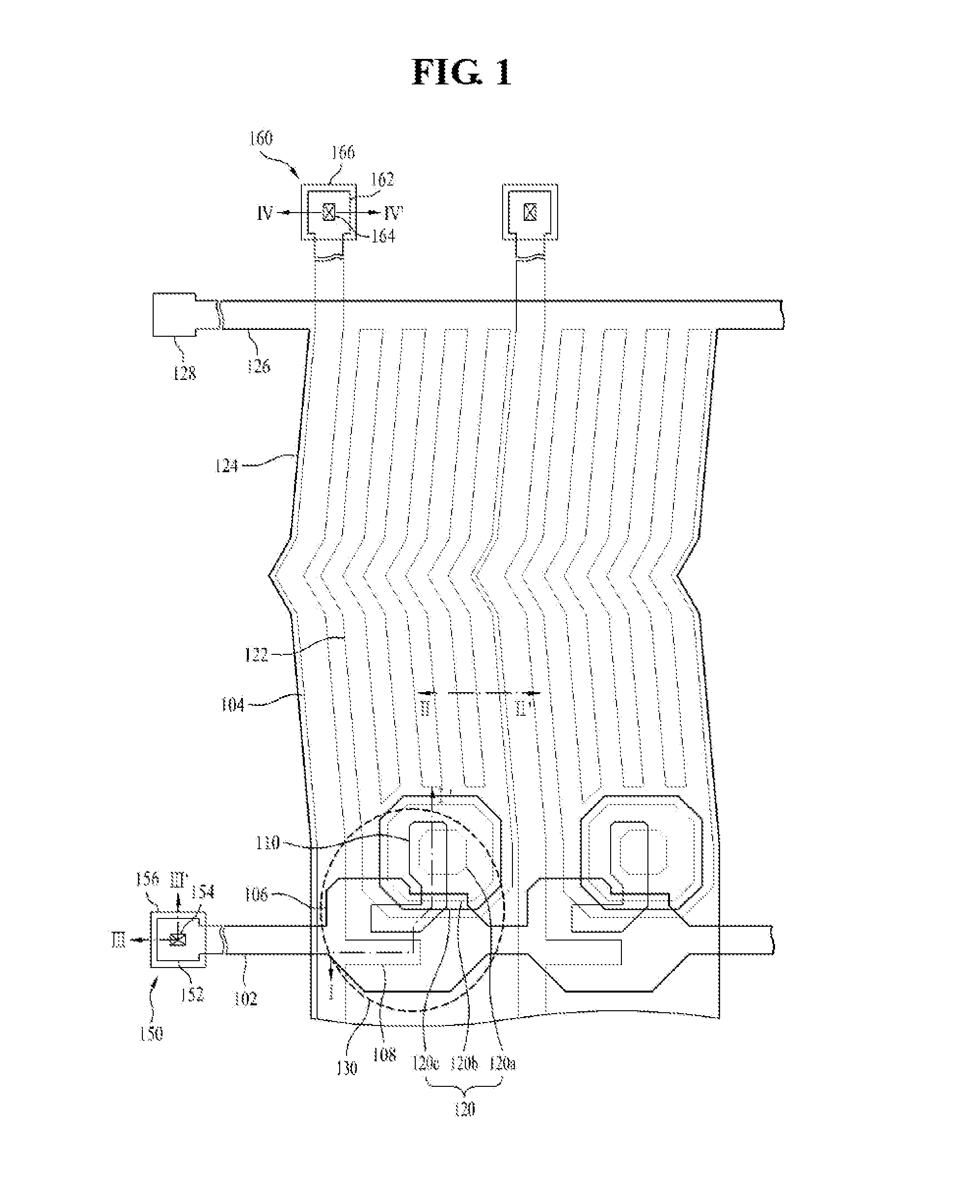
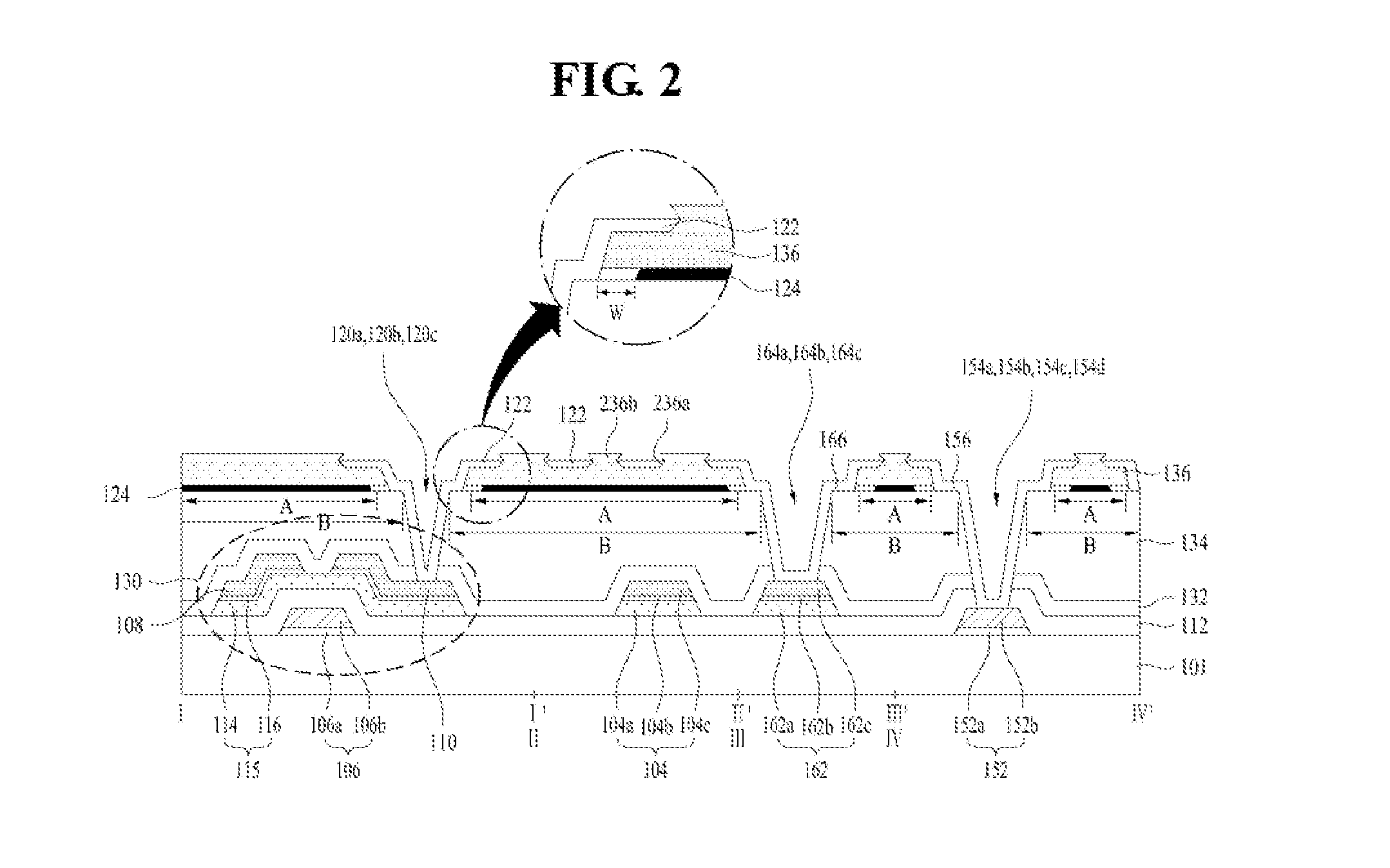
[0041]FIG. 1 is a plan view illustrating a thin film transistor substrate in accordance with one embodiment of the present invention, and FIG. 2 is a cross-sectional view taken along the lines I-I′, II-II′, III-III′ and IV-IV′ of the thin film transistor substr...


PUM


Abstract

Disclosed are a thin film transistor substrate and a method of fabricating the same in which the number of processes is reduced. The method includes forming a first conductive pattern including gate electrodes and gate lines on a substrate through a first mask process, depositing a gate insulating film and forming a second conductive pattern including a semiconductor pattern, source and drain electrodes and data lines through a second mask process, depositing first and second passivation films and forming pixel contact holes passing through the first and second passivation films and exposing the drain electrodes through a third mask process, and forming a third conductive pattern including a common electrode and a common line and forming a third passivation film formed in an undercut structure with the common electrode through a fourth mask process, simultaneously, and forming a fourth conductive pattern including pixel electrodes through a lift-off process.

Description

[0001]This application claims the benefit of Korean Patent Application No. 10-2011-0101959, filed on Oct. 6, 2011, which is hereby incorporated by reference in its entirety.BACKGROUND OF THE INVENTION[0002]1. Field of the Invention[0003]The present invention relates to a thin film transistor substrate and a method of fabricating the same, and more particularly, to a thin film transistor substrate and a method of fabricating the same in which the number of processes is reduced.[0004]2. Discussion of the Related Art[0005]A liquid crystal display device displays an image by adjusting light transmittance of liquid crystals having dielectric anisotropy using an electric field. Such a liquid crystal display device includes a liquid crystal display panel including a thin film transistor substrate and a color filter substrate bonded to each other opposite each other, a backlight unit irradiating light to the liquid crystal display panel, and a driving circuit unit to drive the liquid crysta...

Claims


Application Information

Patent Timeline
Patent Type & Authority Applications(United States)
IPC IPC(8): H01L33/08
CPCH01L27/1288H01L27/02G02F1/1343G02F1/136G02F1/1368
Inventor KWACK, HEE-YOUNG
Owner LG DISPLAY CO LTD
Why Eureka
Try Eureka