Method for fabricating magnetic tunnel junction device

a magnetic tunnel junction and magnetic tunnel technology, applied in the direction of digital storage, instruments, electrical equipment, etc., can solve the problems of difficult to fabricate a semiconductor device including an mtj element, difficult to pattern materials constituting an mtj element, and relatively low operating speed of flash memory characterized by non-volatility and high degree of integration, so as to reduce the number of processes to be performed

Active Publication Date: 2013-02-07
SAMSUNG SEMICON +1
View PDF17 Cites 39 Cited by
  • Summary
  • Abstract
  • Description
  • Claims
  • Application Information

AI Technical Summary

Benefits of technology

[0010]An embodiment of the present invention is directed to a method for fabricating a semiconductor device including a magnetic tunnel junction device, which may decrease the number of processes to be performed.
[0011]In accordance with an embodiment of the present invention, a method for fabricating a semiconductor device includes forming a plurality of layers which are stacked as a bottom layer, a magnetic tunnel junction (MTJ) layer, and a top layer, patterning the top layer and the MTJ layer using an etch mask pattern to form a top layer pattern and an MTJ pattern, forming a carbon spacer on the sidewalls of the MTJ pattern and the top layer pattern to protect the MTJ pattern and the top layer pattern, and patterning the bottom layer using the carbon spacer and the etch mask pattern as an etch mask to form a bottom layer pattern.

Problems solved by technology

Also, a flash memory characterized by non-volatility and high degree of integration may have a relatively low operating speed.
Here, it is difficult to pattern materials constituting an MTJ element, in a general process for manufacturing a semiconductor.
Since electrode layers disposed over and under an MTJ element are to be patterned by a different patterning process from that of the MTJ element, it becomes more difficult to fabricate a semiconductor device including an MTJ element.
Therefore, a manufacturing process of the semiconductor device may be more complicated.

Method used


Image

  • Method for fabricating magnetic tunnel junction device
  • Method for fabricating magnetic tunnel junction device
  • Method for fabricating magnetic tunnel junction device

Examples


Embodiment Construction

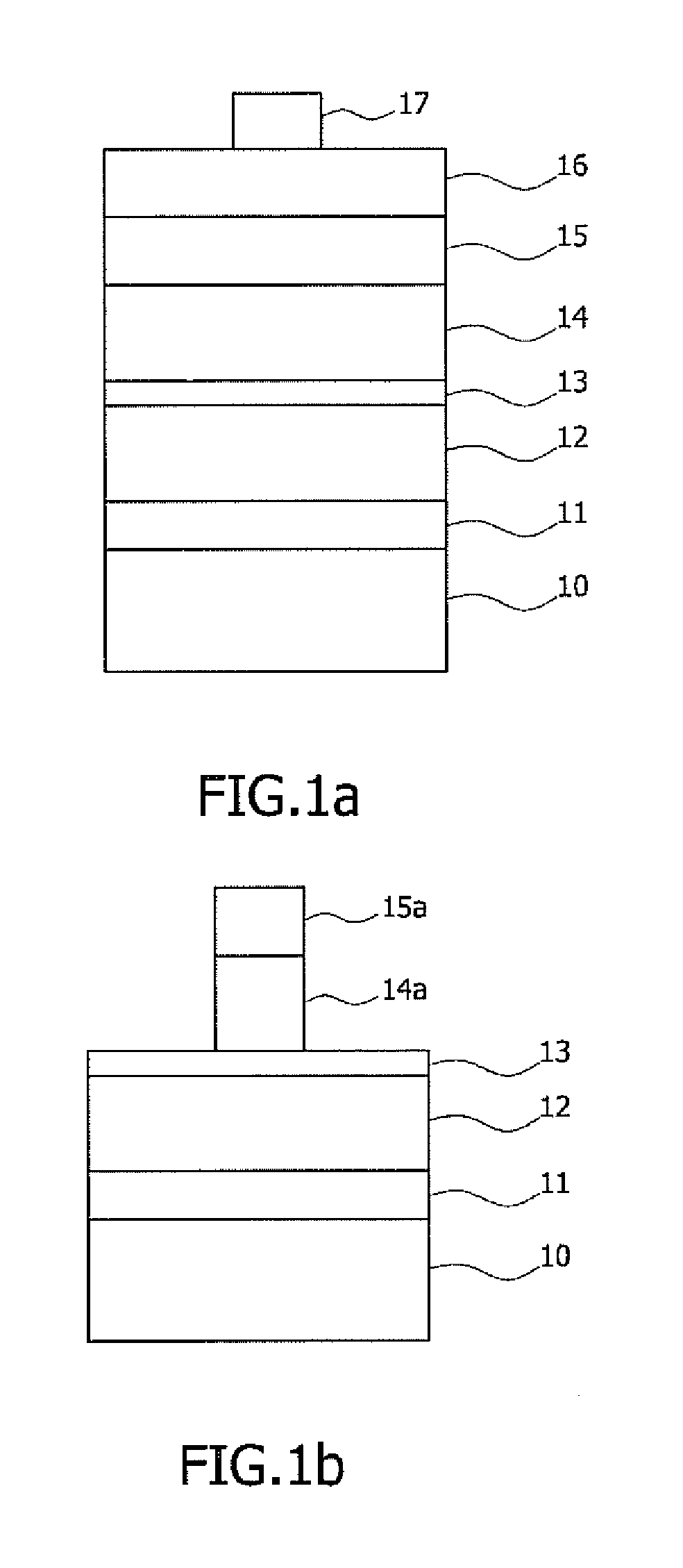
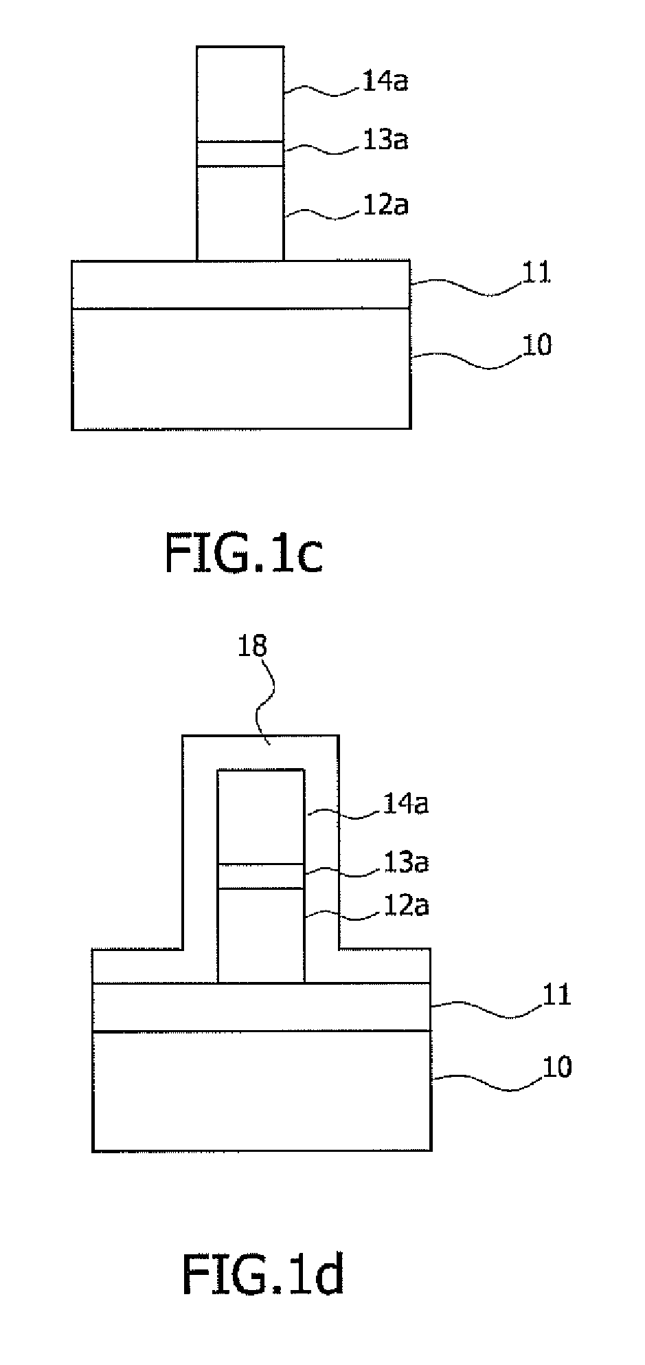
[0016]Exemplary embodiments of the present invention will be described below in more detail with reference to the accompanying drawings. The present invention may, however, be embodied in different forms and should not be construed as limited to the embodiments set forth herein. Rather, these embodiments are provided so that this disclosure will be thorough and complete, and will fully convey the scope of the present invention to those skilled in the art. Throughout the disclosure, like reference numerals refer to like parts throughout the various figures and embodiments of the present invention.

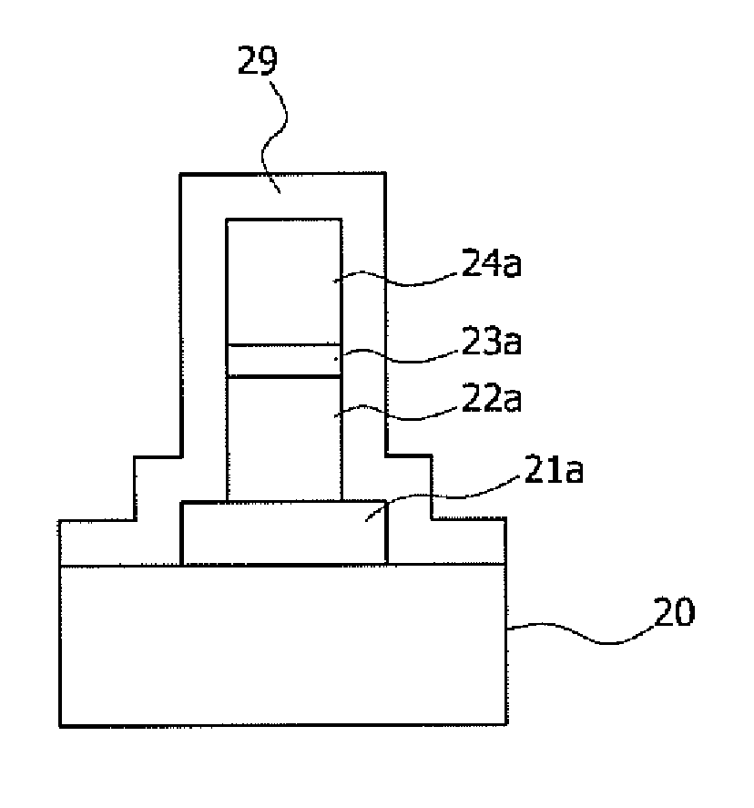
[0017]In an embodiment of the present invention, a carbon spacer is formed by an in-situ process using a carbon-containing etching gas during an etching process of an MTJ element. The carbon spacer might be a carbon polymer spacer. A nitride spacer deposition process in a low temperature and an etching process using the nitride spacer deposition as a mask according to the conventional art mi...


PUM


Abstract

A method for fabricating a semiconductor device includes forming a plurality of layers which are stacked as a bottom layer, an MTJ layer, and a top layer, patterning the top layer and the MTJ layer using an etch mask pattern to form a top layer pattern and an MTJ pattern, forming a carbon spacer on the sidewalls of the MTJ pattern and the top layer pattern to protect the MTJ pattern and the top layer pattern, and patterning the bottom layer using the carbon spacer and the etch mask pattern as an etch mask to form a bottom layer pattern.

Description

CROSS-REFERENCE TO RELATED APPLICATIONS[0001]The present application claims priority of Korean Patent Application No. 10-2011-0077616, filed on Aug. 4, 2011, which is incorporated herein by reference in its entirety.BACKGROUND[0002]1. Field[0003]Exemplary embodiments of the present invention relate to a device used in an integrated circuit, and more particularly, to a magnetic tunnel junction device.[0004]2. Description of the Related Art[0005]A dynamic random access memory (DRAM) is an exemplary memory device which has been widely used. A DRAM has a feature of operating at a high speed and may be highly integrated. Here, a DRAM is a volatile memory loses data when power is interrupted, and a refresh operation is to be performed to rewrite data periodically.[0006]Also, a flash memory characterized by non-volatility and high degree of integration may have a relatively low operating speed. A magnetoresistive memory device which stores data using a magneto-resistance change may be fabr...

Claims


Application Information

Patent Timeline
Patent Type & Authority Applications(United States)
IPC IPC(8): H01L43/12
CPCH01L43/12G11C11/161H10N50/01G11C11/15
Inventor LEE, MIN SUK
Owner SAMSUNG SEMICON
Why Eureka
Try Eureka