Pixel structure
A technology of pixel structure and metal layer, applied in the field of pixel structure, can solve the problems of complicated pixel structure process and so on
- Summary
- Abstract
- Description
- Claims
- Application Information
AI Technical Summary
Problems solved by technology
Method used
Image

Examples
Embodiment Construction
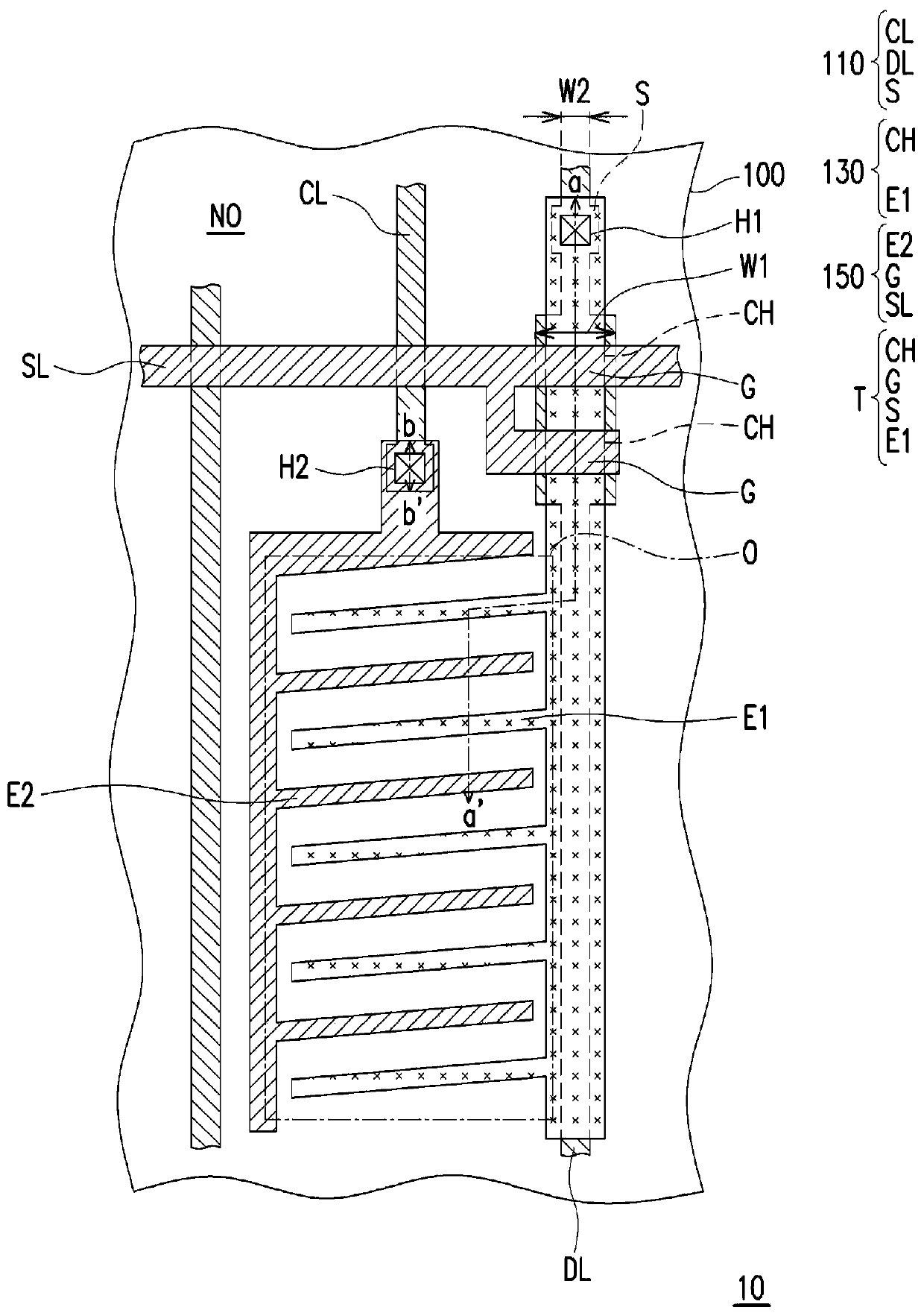
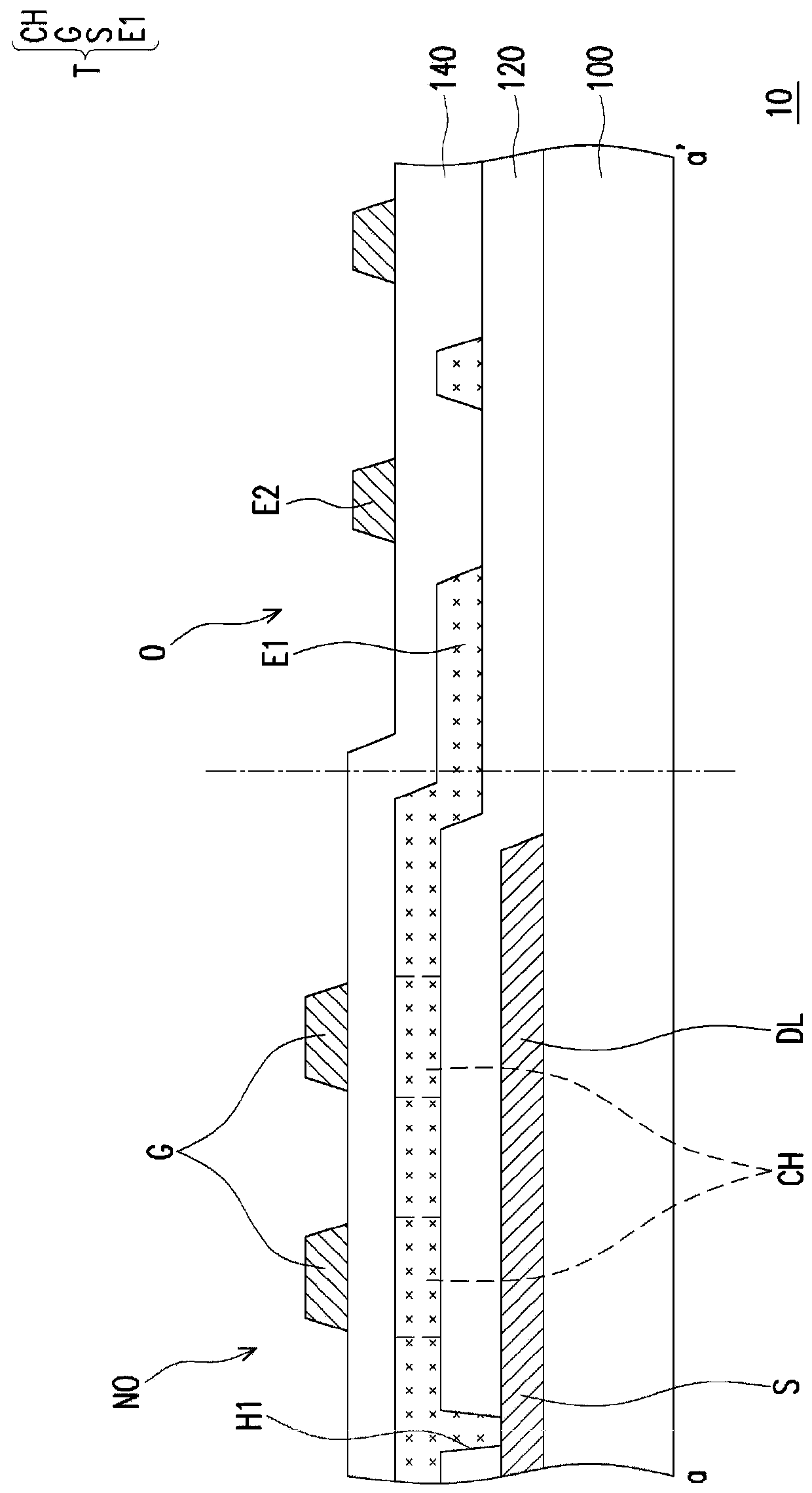
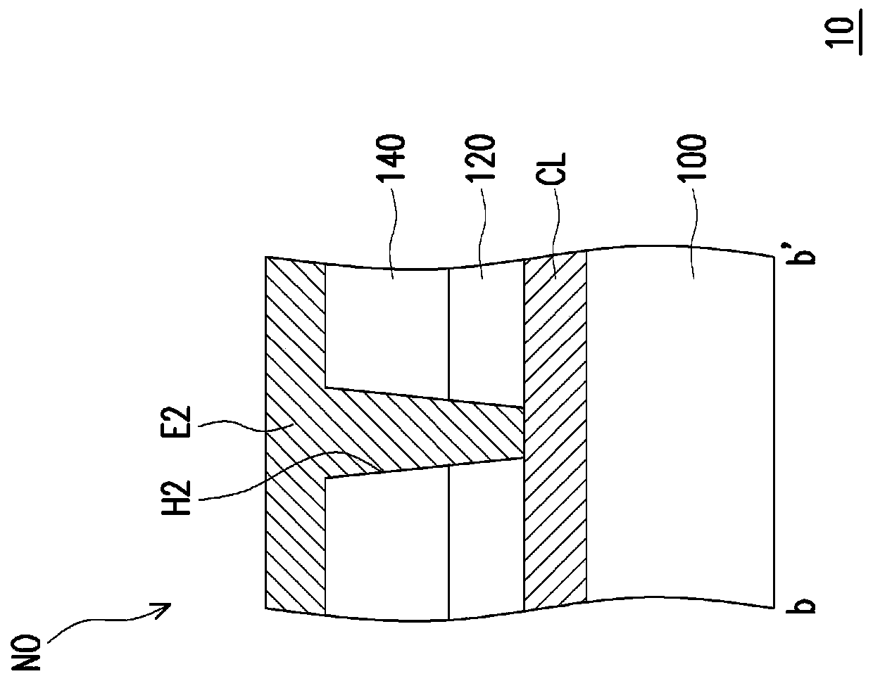
[0034] Figure 1A It is a top view of a pixel structure according to an embodiment of the present invention. Figure 1B yes Figure 1A Schematic cross-sectional view of section line aa'. Figure 1C yes Figure 1A Schematic cross-sectional view of section line bb'.
[0035] Please refer to Figure 1A to Figure 1C The pixel structure 10 includes a substrate 100 , a first metal layer 110 , a first insulating layer 120 , a conductive layer 130 , a second insulating layer 140 and a second metal layer 150 . In this embodiment, the pixel structure 10 includes an opening area O and a non-opening area NO around the opening area O. As shown in FIG. In some embodiments, a black matrix (not shown) overlaps the non-opening area NO, and the black matrix has through holes corresponding to the opening area O. Referring to FIG.
[0036] The first metal layer 110 is located on the substrate 100 . The first metal layer 110 includes a data line DL and a source S connected to the data line DL....
PUM
 Abstract
Description
Claims
Application Information
 - R&D
- Intellectual Property
- Life Sciences
- Materials
- Tech Scout
- Unparalleled Data Quality
- Higher Quality Content
- 60% Fewer Hallucinations
Browse by: Latest US Patents, China's latest patents, Technical Efficacy Thesaurus, Application Domain, Technology Topic, Popular Technical Reports.
© 2025 PatSnap. All rights reserved.Legal|Privacy policy|Modern Slavery Act Transparency Statement|Sitemap|About US| Contact US: help@patsnap.com