TOUCH PANEL and display device

A touch panel and conductor wire technology, which is applied in the field of display devices, can solve the problems of difficulty in suppressing contractures and moire fringes, and achieves the effect of suppressing moiré fringes.

Pending Publication Date: 2019-10-22
VTS TOUCHSENSOR CO LTD
View PDF5 Cites 0 Cited by
  • Summary
  • Abstract
  • Description
  • Claims
  • Application Information

AI Technical Summary

Problems solved by technology

[0005] In the technique described in Patent Document 1, if the amount of displacement for shifting the positions of the vertices at which two thin metal wires intersect each other is too small, there is a problem that it is difficult to suppress moire fringes.
In addition, if the amount of displacement for shifting the position of the apex is too large, there is a problem that it is difficult to suppress the occurrence of twine grains.

Method used


Image

  • TOUCH PANEL and display device
  • TOUCH PANEL and display device
  • TOUCH PANEL and display device

Examples


no. 1 approach

[0026] Hereinafter, a first embodiment of the present invention will be described with reference to the drawings.

[0027] (constitute)

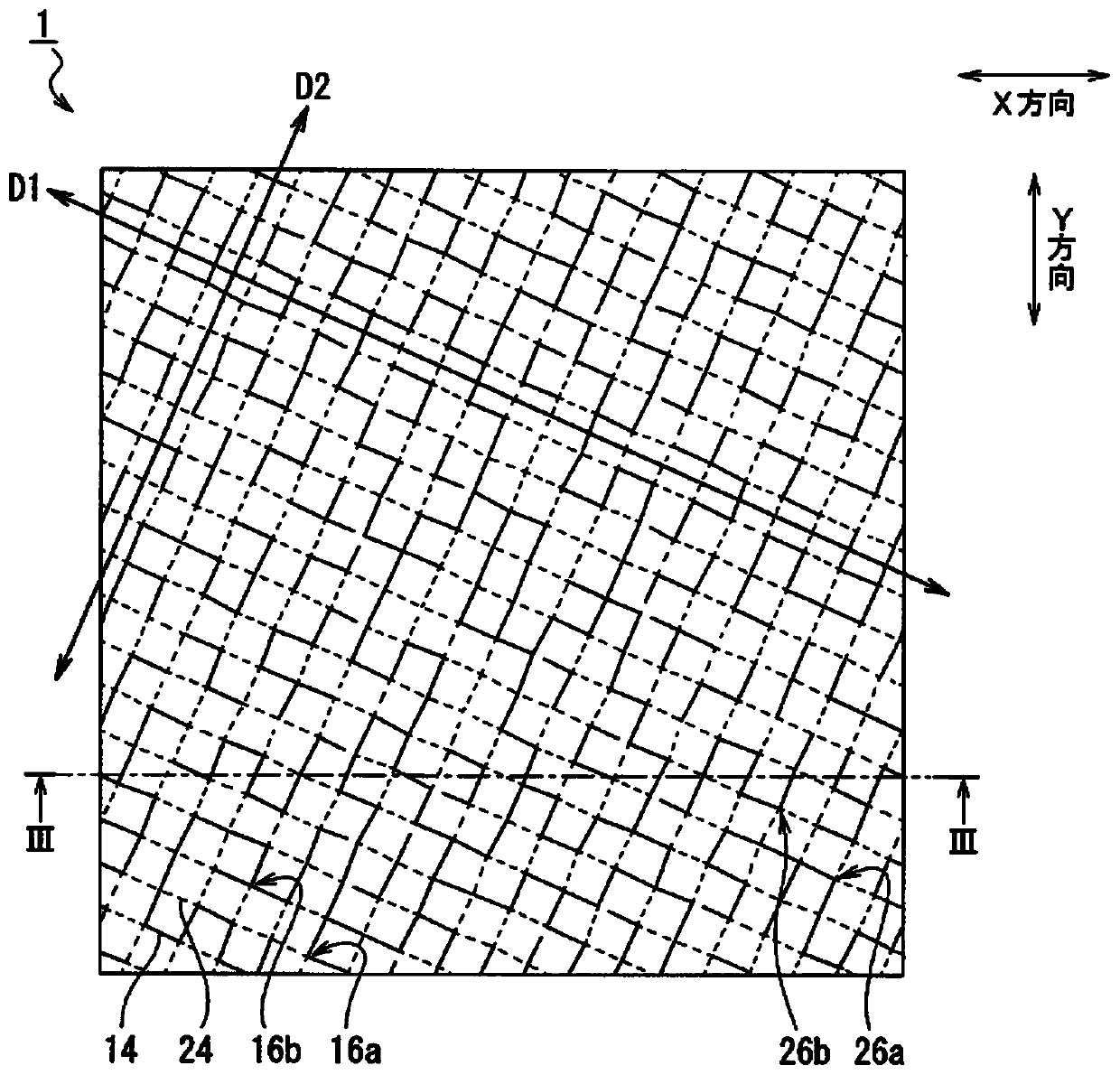
[0028] refer to Figure 1 to Figure 8 , the configuration of the touch panel 1 will be described.

[0029] (Schematic configuration of touch panel 1)

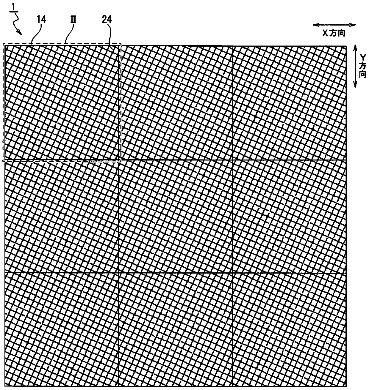
[0030] Figure 1 to Figure 3 The touch panel 1 shown in is arranged, for example, in a car navigation system or the like.

[0031] In addition, the touch panel 1 is a panel having a plurality of detection regions corresponding to a plurality of coordinates, and is, for example, a capacitive touch panel.

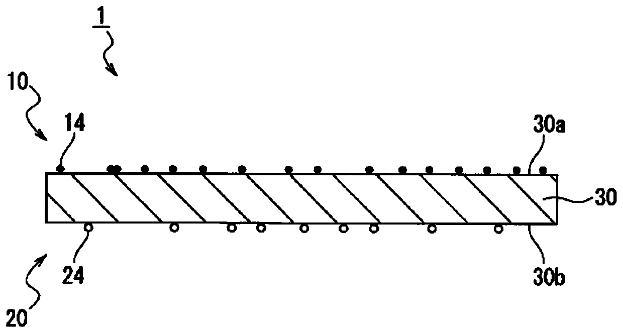
[0032] In addition, the touch panel 1 is a panel laminated on a display panel (display device) such as a liquid crystal panel via an adhesive member.

[0033] In addition, in figure 1 shows nine detection areas in the detection area of ​​the touch panel 1, and the nine detection areas correspond to the three coordinates arranged in the vertical direction (capacitance detection unit: no...

Embodiment 1

[0148] The touch panel of Example 1 is a touch panel in which the portion where the conductor lines intersect in each of the first conductive layer and the second conductive layer is less than 10% of the portion corresponding to all the vertices of the imaginary quadrilateral.


PUM


Abstract

The problem addressed by the present invention lies in providing a touch panel capable of suppressing the occurrence of moire without causing graining to occur, and a display device onto which the touch panel has been stacked. In order to solve this problem, a touch panel is provided with a first electrically conductive layer including a plurality of conductor wires, and a second electrically conductive layer including a plurality of conductor wires, wherein: in a plan view in a state in which the first electrically conductive layer and the second electrically conductive layer are stacked on one another, a pattern of continuously arranged virtual quadrilaterals VS, which are virtual quadrilaterals having the same shape, formed by the first conductor wires and the second conductor wires, isdefined as a reference pattern; in the first electrically conductive layer and the second electrically conductive layer respectively, parts where the conductor wires intersect constitute less than 10% of virtual vertices VP, which are the parts corresponding to all virtual vertices of the virtual quadrilaterals VS; and in a plan view, each actual vertex CP, which is a vertex formed by the two conductor wires, is disposed in a position displaced by an amount of displacement at least equal to 1% and less than 50% of the length of a pitch WP, which is the length of one side of the virtual quadrilateral VS, from the virtual vertex VP.

Description

technical field [0001] The present invention relates to a touch panel laminated on a display device, such as a touch panel included in a portable communication terminal, and a display device laminated with the touch panel. Background technique [0002] As a technique for forming a pattern with thin metal wires (metal thin wires) on a touch panel included in a display device, there is a technique described in Patent Document 1, for example. [0003] In the technique of Patent Document 1, the translucent support has translucent sensor parts extending in the first direction, and the sensor parts are arranged alternately in the second direction, which is a direction perpendicular to the first direction. Dummy part of translucency. Furthermore, the sensor portions are arranged at a period L in the second direction, the sensor portion and the dummy portion are composed of a mesh-like fine metal wire pattern, and at least a part of the fine metal wire pattern in the sensor portion...

Claims


Application Information

Patent Timeline
Patent Type & Authority Applications(China)
IPC IPC(8): G06F3/041G06F3/044
CPCG06F3/0412G06F3/044G06F3/0445G06F2203/04112G06F3/047G06F2203/04104
Inventor 伴井香苗原田贵浩史薇
Owner VTS TOUCHSENSOR CO LTD
Why Eureka
Try Eureka