
Packaging structure based on quantum dots, and display

A technology of packaging structure and quantum dots, applied in the direction of electric solid devices, semiconductor devices, electrical components, etc., can solve the problem of uneven color display, and achieve the effect of eliminating the coffee ring effect, convenient operation and uniform display.

Active Publication Date: 2019-10-22
SHENZHEN INSTITUTE OF INFORMATION TECHNOLOGY +1
View PDF4 Cites 2 Cited by
  • Summary
  • Abstract
  • Description
  • Claims
  • Application Information

AI Technical Summary

Problems solved by technology

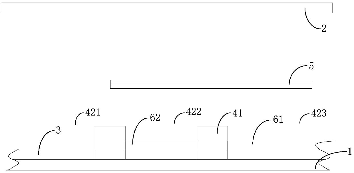
[0004] The purpose of the present invention is to provide a packaging structure and display based on quantum dots, which aims to solve the technical problem in the prior art that the coffee ring effect is likely to occur when quantum dots are inkjet printed on Micro LEDs, resulting in uneven color display.

Method used


Image

  • Packaging structure based on quantum dots, and display
  • Packaging structure based on quantum dots, and display
  • Packaging structure based on quantum dots, and display

Examples


Embodiment Construction

[0032] The following describes in detail the embodiments of the present invention, examples of which are illustrated in the accompanying drawings, wherein the same or similar reference numerals refer to the same or similar elements or elements having the same or similar functions throughout. The embodiments described below with reference to the accompanying drawings are exemplary, and are intended to explain the present invention and should not be construed as limiting the present invention.

[0033] In the description of the present invention, it should be understood that the terms "length", "width", "upper", "lower", "front", "rear", "left", "right", "vertical", The orientations or positional relationships indicated by "horizontal", "top", "bottom", "inside", "outside", etc. are based on the orientations or positional relationships shown in the accompanying drawings, which are only for the convenience of describing the present invention and simplifying the description, rather...


PUM


Abstract

The invention relates to the technical field of packaging and provides a packaging structure based on quantum dots. The packaging structure comprises a lamp source plate and a plurality of chips arranged on the lamp source plate. The packaging structure also comprises quantum dots and a photoresist layer having adsorption capacity for the quantum dots. The photoresist layer is arranged on the light emitting sides of the chips; a plurality of through grooves are formed in the photoresist layer; the through grooves and the chips are arranged in a one-to-one correspondence mode; the top ends of the chips are connected with the bottom ends of the through grooves and seal the bottom ends of the through grooves; and the quantum dots are arranged at the top ends of the chips in a coating mode andcontained in the through grooves. The invention also provides a display which comprises the packaging structure based on the quantum dots. The photoresist layer with the through grooves is arranged on the chips, the chips and the through grooves are arranged in the one-to-one correspondence manner, and the top ends of the chips are connected with and seal the bottom ends of the through grooves, so that the adsorption force of the side walls of the through grooves can effectively balance the fluid force of the quantum dots, the coffee ring effect is eliminated, the quantum dots in the throughgrooves are more uniformly distributed, and uniform color display is realized.

Description

technical field [0001] The invention relates to the technical field of packaging, and in particular provides a quantum dot-based packaging structure and a display. Background technique [0002] As a new generation of display technology, Micro LED has higher color saturation, better luminous efficiency and lower power consumption than traditional LCD (liquid crystal) and OLED. There are usually two solutions for the display of Micro LED. The first one is to combine red, green and blue (RGB) three-color LED units on the panel. However, the driving circuit is more complicated and difficult to manufacture, and the working voltage of red, green and blue LEDs is different. , the attenuation rate is also different, and the reliability is revealed; the second is to inkjet print light conversion materials on Micro LED chips that are usually smaller than 50 microns, and generate red, green and blue three-color light by exciting the light conversion materials, thereby realizing full-co...

Claims


Application Information

Patent Timeline
Patent Type & Authority Applications(China)
IPC IPC(8): H01L33/50H01L27/15
CPCH01L27/156H01L33/501H01L33/505H01L2933/0041
Inventor 王新中赵志力王恺孙小卫陈明祥
Owner SHENZHEN INSTITUTE OF INFORMATION TECHNOLOGY
Learn More