
Patsnap Eureka
For R&D, Patsnap Eureka makes reading and utilizing patents & technical documents easy.
Patsnap Eureka AIR
Designed for self-driven R&D workflows. Generate viable solutions, solve complex R&D challenges, empower your innovation with AI.

Patsnap Eureka Materials
Designed for material experts only. Revolutionize your material R&D, from search, analyze, to developing new materials.

TechResearch
Generate reliable direction feasibility study reports for your R&D in just a few steps.

TechSeek
Discover and master advanced knowledge NOW. Basics, ideas, possibilities, all at once.

TechMind
As an expert in R&D Theories, TechMind can generates customized viable solutions instantly.

TechRisk
Analyze your overall solution with one click, know your potential R&D risks in advance.

TechMonitor
Get weekly tech updates, stay abreast of the latest tech innovations and key insights.
Micro light emitting diode transfer substrate and device
A technology of micro-light-emitting diodes and transfer substrates, which is applied to semiconductor devices, electrical components, circuits, etc., can solve the problems of large spacing between micro-light-emitting diodes, inability to meet the high-precision requirements of mass transfer, and low accuracy
- Summary
- Abstract
- Description
- Claims
- Application Information
AI Technical Summary
Problems solved by technology
Method used
Image

Examples
Embodiment 1
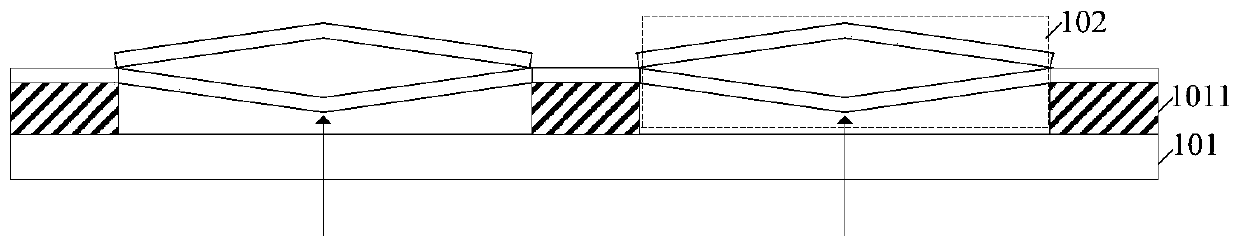
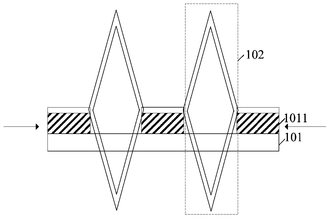
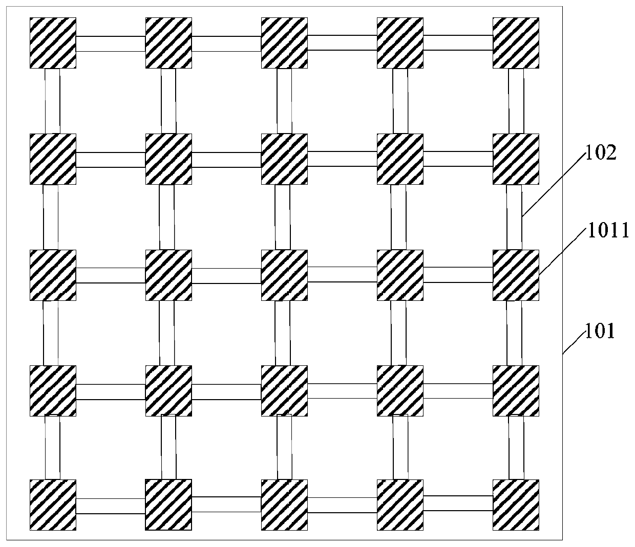
[0027] An embodiment of the present invention provides a transfer substrate for micro-light emitting diodes, which can be used for mass transfer of micro-light-emitting diodes in the process of manufacturing micro-light-emitting diode display panels, Figure 1a with Figure 1b A schematic diagram of a side-view structure of a micro-LED transfer substrate provided in an embodiment of the present invention, as shown in Figure 1a with Figure 1b As shown, the micro light emitting diode transfer substrate provided by the embodiment of the present invention includes: a base 101 and a distance adjustment unit 102 . The base 101 has a plurality of bases 1011 arranged at intervals; the bases 1011 are used to carry the micro light-emitting diodes to be transferred; the distance adjustment unit 102 is arranged between two adjacent bases 1011 for adjusting the distance between the bases 1011 .
[0028] In the initial state of the micro light-emitting diode transfer substrate provided b...
Embodiment 2
[0045] Based on the same inventive concept, an embodiment of the present invention provides a micro-LED transfer device, the micro-LED transfer transposition includes the micro-LED transfer substrate provided in the above embodiment, and also includes a push module, the push module and the distance adjustment unit The connection is used to apply an external force to the distance adjustment unit, so that the distance adjustment unit can adjust the distance between the bases.
[0046] It should be noted that the push module can apply external force to the micro-LED transfer substrate, so that the distance adjustment unit is in a stretched or contracted state, so the distance between adjacent bases can be shortened, thereby shortening the distance between the micro-light-emitting diodes to be transferred. The distance between them can further improve the accuracy of the mass transfer of micro-light emitting diodes, and realize the high-precision mass transfer of micro-light-emitti...
PUM
 Abstract
Description
Claims
Application Information
 - R&D Engineer
- R&D Manager
- IP Professional
- Industry Leading Data Capabilities
- Powerful AI technology
- Patent DNA Extraction
Browse by: Latest US Patents, China's latest patents, Technical Efficacy Thesaurus, Application Domain, Technology Topic, Popular Technical Reports.
© 2024 PatSnap. All rights reserved.Legal|Privacy policy|Modern Slavery Act Transparency Statement|Sitemap|About US| Contact US: help@patsnap.com