Unlock instant, AI-driven research and patent intelligence for your innovation.

Erase method for flash memory

A technology of flash memory and storage unit, applied in the field of erasing of flash memory, which can solve the problem of time-consuming erasure verification

Active Publication Date: 2021-09-14
ELITE SEMICON MEMORY TECH INC
View PDF7 Cites 0 Cited by
  • Summary
  • Abstract
  • Description
  • Claims
  • Application Information

AI Technical Summary

Problems solved by technology

This known erasure method requires multiple additional tag buffers and consumes more erasure verification time

Method used


Image

  • Erase method for flash memory
  • Erase method for flash memory
  • Erase method for flash memory

Examples


Embodiment Construction

[0026] In order to fully understand the purpose, features and effects of the present invention, the present invention will be described in detail by means of the following specific embodiments and accompanying drawings, as follows.

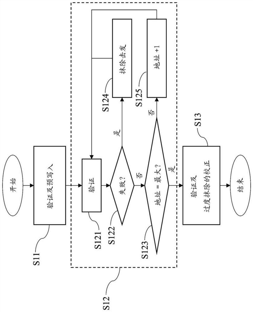
[0027]An embodiment of the present disclosure provides an erasing method for a flash memory. In the verification and erasing steps, an erasing shot is injected into all transistor memory cells of a memory block (that is, erasing the memory area After removing all transistor memory cells of the block), the provided erase method verifies whether the memory block has at least one over-erased transistor memory cell. When a memory block has at least one over-erased transistor memory cell, the provided erase method injects the erase shot into a plurality of transistor memory cells in the memory block (that is, erases all transistor memory cells in the memory block ), and then, the provided erase method verifies whether all transistor memory cells of the...


PUM


Abstract

A method for erasing a flash memory is illustrated as follows, wherein the flash memory includes at least one storage block, and the storage block is divided into a plurality of storage segments. Verifying whether a memory block or a memory block corresponding to an address has at least one under-erased transistor memory cell according to a sector enable signal, wherein the sector enable signal depends on whether the memory block has at least one over-erased transistor memory cell unit is determined. If the storage block or storage segment corresponding to the address has transistor memory cells that are insufficient to be erased, the transistor storage cells of the storage block or storage segment are erased according to the segment enable signal.

Description

technical field [0001] The present invention relates to a flash memory, more particularly to an erasing method for the flash memory. Background technique [0002] Flash memory includes a plurality of individual metal oxide semiconductor (MOS) field effect transistor memory cells, each transistor memory cell including a source, a drain, a floating gate, and a control gate. Various voltages can be applied to the above-mentioned plurality of electrodes of the transistor memory cell to program (that is, write) the transistor memory cell into binary 1 or 0, erase all transistor memory cells as a memory block, and read transistor memory cells. memory cells, verify that the transistor memory cells are erased, or verify that the transistor memory cells are not over-erased. [0003] The adverse effect of the leakage current of an over-erased transistor memory cell is described as follows. In a typical flash memory, the drains of a large number of transistor memory cells, for exampl...

Claims


Application Information

Patent Timeline
Patent Type & Authority Patents(China)
IPC IPC(8): G11C16/16
CPCG11C16/16
Inventor 陈致豪
Owner ELITE SEMICON MEMORY TECH INC