Dual-array package light source structure and packaging method thereof

A light source and installation groove technology, which is applied to electrical components, electrical solid devices, circuits, etc., can solve the problems of complex LED chip packaging procedures, heat generated by LED chips, and low processing efficiency, so as to improve the dustproof effect and heat dissipation speed , the effect of prolonging the service life

Active Publication Date: 2019-11-08
广东良友科技有限公司
View PDF4 Cites 5 Cited by
  • Summary
  • Abstract
  • Description
  • Claims
  • Application Information

AI Technical Summary

Problems solved by technology

[0004] The purpose of the present invention is to provide a double-array array package light source structure and packaging method to solve the problem mentioned in the background art that most of the LED chips now use a single array array, and the brightness is poor. The LED chips will generate heat when they are used, and need to be processed. , LED chip packaging procedures are complicated and the processing efficiency is low

Method used


Image

  • Dual-array package light source structure and packaging method thereof
  • Dual-array package light source structure and packaging method thereof
  • Dual-array package light source structure and packaging method thereof

Examples


Embodiment 1

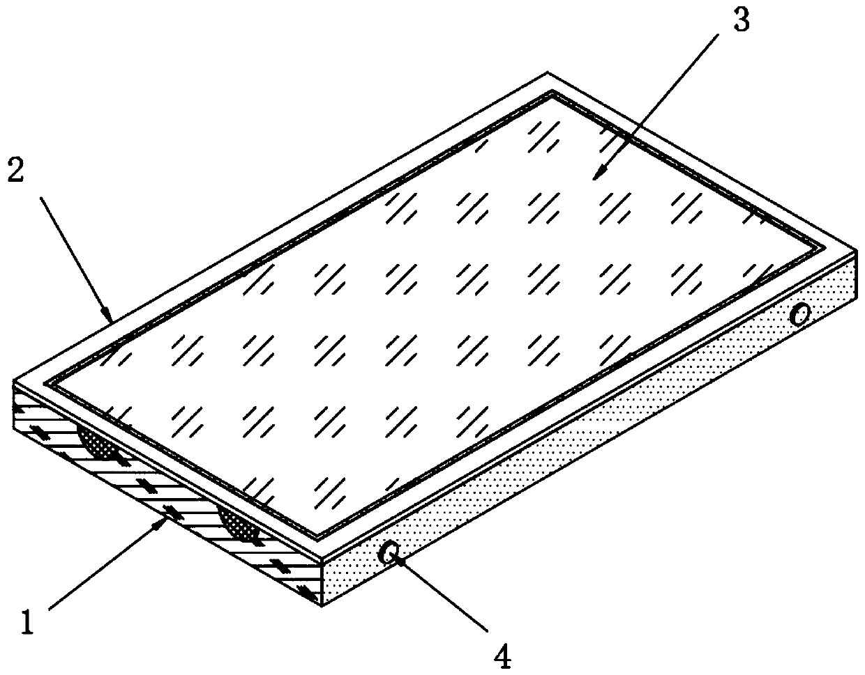
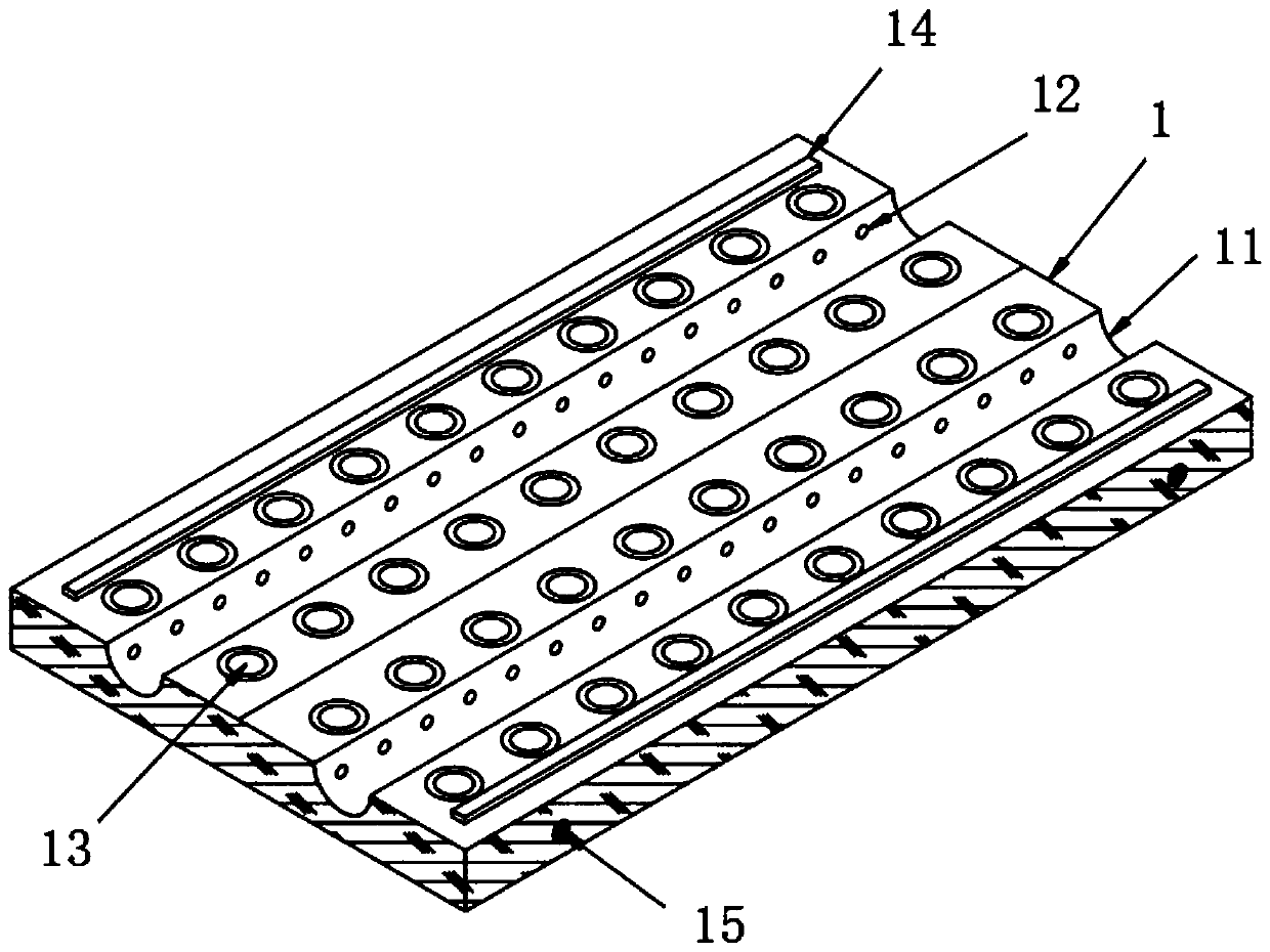
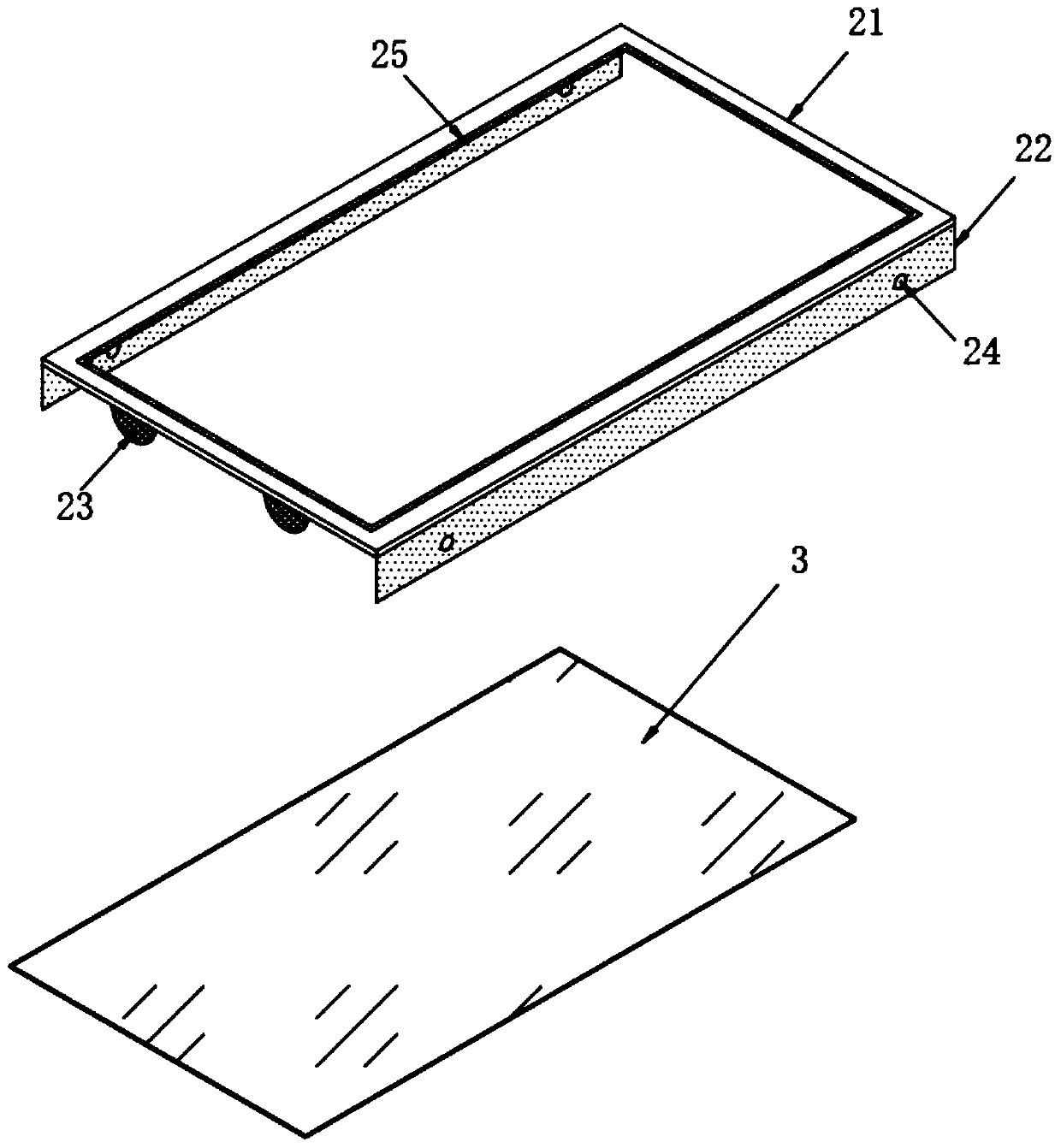
[0031] A double-array packaged light source structure, such as figure 1 and figure 2 As shown, it includes a cuboid substrate 1, two symmetrical cooling grooves 11 are provided on the top surface of the substrate 1, and the cross section of the cooling grooves 11 is semicircular. A distance from the LED chips 13 arranged linearly, a heat dissipation through hole 12 is opened on the inner wall of each heat dissipation groove 11, and each LED chip 13 is provided with a mounting groove, and the LED chip 13 is snap-fitted with the mounting groove, and the heat dissipation through hole 12 communicates with the inside of the installation groove, and both sides of the substrate 1 are symmetrically provided with threaded holes 15; the top of the substrate 1 is provided with an isolation frame 2, and a glass sheet 3 is arranged between the isolation frame 2 and the substrate 1, such as image 3 As shown, the isolation frame 2 includes a frame 21, the frame 21 is a square ring structu...

Embodiment 2

[0045] As a second embodiment of the present invention, both sides of the top surface of the substrate 1 are symmetrically provided with damping strips 14 , and the sum of the thicknesses of the damping strips 14 and the glass sheet 3 is equal to the thickness of the frame 21 .

[0046] Further, the shock absorbing strip 14 is made of high temperature resistant rubber material.

[0047] Specifically, the width between the two damping strips 14 is smaller than the width of the glass sheet 3 .

[0048] In the double-array packaged light source structure of this embodiment, shock absorbing strips 14 are arranged symmetrically on both sides of the top surface of the substrate 1 , so that the structure of the glass sheet 3 is more stable when installed.


PUM


Abstract

The invention relates to the technical field of LED production, in particular to a dual-array package light source structure and a packaging method thereof. The dual-array package light source structure comprises a substrate, two symmetric heat dissipation slots are arranged on the top surface of the substrate, LED chips are symmetrically arranged at two sides of each heat dissipation slot, the inner wall of the each heat dissipation slot is provided with a heat dissipation through hole, each LED chip is provided with a mounting groove, threaded holes are symmetrically arranged at the two sides of the substrate; the top portion of the substrate is provided with an isolation frame, a glass sheet is arranged between the isolation frame and the substrate, the isolation frame comprises a frame, and fixed plates are symmetrically arranged at the two sides of the frame. The dual-array LED chips are arranged to improve the light emitting speed and improve the brightness; by arranging the heatdissipation slots and the heat dissipation through holes and communicating the heat dissipation through holes with the mounting grooves in the LED chips, the heat dissipation speed of the LED chips is improved, the service life is prolonged, the maintenance cost is reduced, the fixed plates pass through the fixed holes and the threaded holes in order through fixed bolts to be connected on the substrate to facilitate fixing of the glass sheet and facilitate mounting and dismounting.

Description

technical field [0001] The invention relates to the technical field of LED production, in particular to a double-array packaged light source structure and a package method. Background technique [0002] A light-emitting diode (Light-EmittingDiode, LED) is a semiconductor electronic component capable of emitting light. This electronic component appeared as early as 1962. In the early days, it could only emit red light with low luminosity. Later, other monochromatic light versions were developed. Today, the light that can be emitted has covered visible light, infrared rays and ultraviolet rays, and the luminosity has also increased to a considerable extent. of luminosity. And the use is also used as indicator lights, display panels, etc. from the beginning; with the continuous advancement of technology, light-emitting diodes have been widely used in displays, TV lighting decoration and lighting. [0003] There are many packaging methods for LEDs. At present, a common packagi...

Claims


Application Information

Patent Timeline
Patent Type & Authority Applications(China)
IPC IPC(8): H01L25/075H01L33/48H01L33/64
CPCH01L25/0753H01L33/48H01L33/642H01L2933/0033
Inventor 廖建文
Owner 广东良友科技有限公司
Why Eureka
Try Eureka