Polarization microstructure Micro-LED and application thereof in naked eye 3D display system

A display system and microstructure technology, applied in the direction of instruments, electrical components, circuits, etc., can solve the problems of high price, high production cost of cylindrical lens grating, limited application, etc. The effect of high-definition picture

Inactive Publication Date: 2020-12-04
CENT SOUTH UNIV
View PDF3 Cites 0 Cited by
  • Summary
  • Abstract
  • Description
  • Claims
  • Application Information

AI Technical Summary

Problems solved by technology

[0005] However, the production cost of the cylindrical lens grating is high, mainly because the mold for manufacturing the grating is expensive, so the requirements for the accuracy of the design are relatively strict, and the application in the market is also limited.

Method used


Image

  • Polarization microstructure Micro-LED and application thereof in naked eye 3D display system
  • Polarization microstructure Micro-LED and application thereof in naked eye 3D display system
  • Polarization microstructure Micro-LED and application thereof in naked eye 3D display system

Examples


Embodiment 1

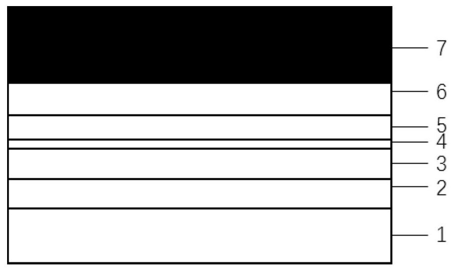
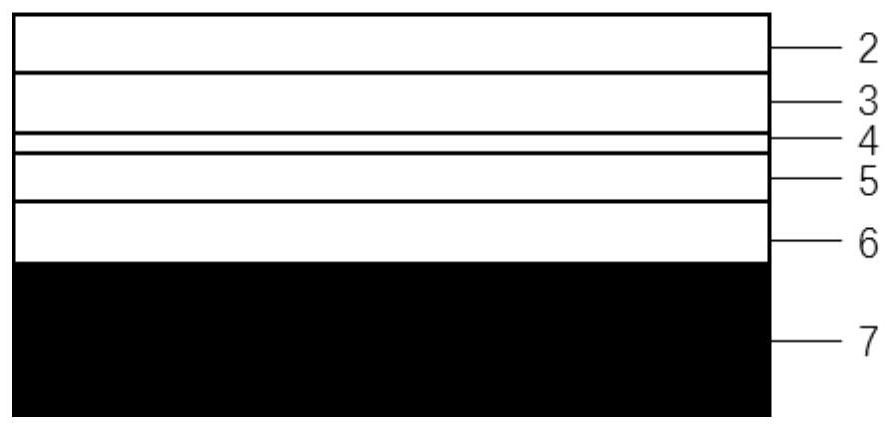
[0053] Such micro-structure of the present invention, such as Micro-LED infrastructures Figure 9 Shown, from bottom to top comprises a metal substrate 7, a conductive layer 6, a nitride layer 5, a multi-quantum well active layer 4, two nitride layer 3, an oxide DBR10, polarizing microstructured surface 12. The width of the metal substrate and the conductive layer 7 is equal to 6; the width of a nitride layer 5 is smaller than the conductive layer 6, a nitride layer 5, a multi-quantum well active layer 4, the width of the two nitride layers 3 are equal, so that nitrogen 5 a layer of a multiple quantum well active layer 4, the nitride layer 3 may be two two mesas 11 are exposed at both sides of its flat sidewall leakage, the conductive layer 6; the width is less than the nitrogen oxide DBR10 3 of two layers, the two ends of the nitride layer 3 will leak out table 11, with a passivation layer 8 on the table 11 and the side walls; the passivation layer is provided on the side of the o...

Embodiment 2

[0057] Preparation of the microstructure of the blue region of Micro-LED emission wavelength belongs:

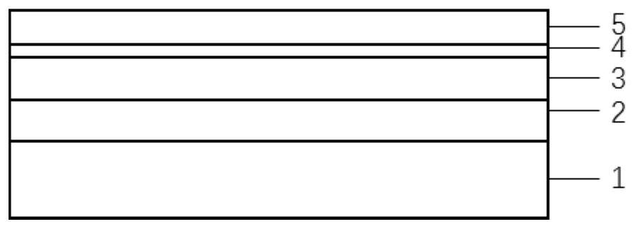
[0058] (1) on the (0001) plane sapphire (substrate 1) are sequentially grown by the MOCVD method u-GaN layer 2 (thickness of 5μm), two of the nitride layer 3 (made of n-GaN, having a thickness of 5μm), [ InGaN (2nm) / GaN (10nm)] 8 The MQW (Quantum Well) layer 4 (having a thickness of 96 nm), a nitride layer, a 5 (material of p-GaN, having a thickness of 100 nm or), obtained LED epitaxial material, the emission wavelength of the MQW (Quantum Well) the In group 4 layers parts by mass percentage of 15%; in the embodiment of the present embodiment is a light emission wavelength 470nm, it belongs to the blue region, the structure of LED epitaxial material obtained in step (1) as figure 1 Indicated.

[0059] (2) electron beam evaporation method of fabricating a conductive layer on the nitride layer 6 is a 5, wherein the deposition temperature is 220 deg.] C, the conductive layer is a...

Embodiment 3

[0070] Preparation of the green region of the microstructure of Micro-LED emission wavelength belongs:

[0071] (1) on the (0001) plane sapphire (substrate 1) are sequentially grown by the MOCVD method u-GaN layer 2 (thickness of 5μm), two of the nitride layer 3 (made of n-GaN, having a thickness of 5μm), [ InGaN (2nm) / GaN (10nm)] 8 The MQW (Quantum Well) layer 4 (96 nm thick), a nitride layer 5 (made of p-GaN with a thickness of 100 nm or), obtained LED epitaxial material, the emission wavelength of the MQW (Quantum Well) layer 4 In composition mass percentage of 28%, in the present embodiment, the light emitting wavelength of 525nm, belonging to green region. LED epitaxial structure material obtained in step (1) as figure 1 Indicated.

[0072] (2) electron beam evaporation method of fabricating a conductive layer on the nitride layer 6 is a 5, wherein the deposition temperature is 220 deg.] C, the conductive layer is an ITO, thickness of the conductive layer 6 is 280nm.

[007...


PUM

PropertyMeasurementUnit
thicknessaaaaaaaaaa
thicknessaaaaaaaaaa
thicknessaaaaaaaaaa

Abstract

The invention discloses a polarization microstructure Micro-LED and application thereof in a naked eye 3D display system. The polarization microstructure Micro-LED structurally comprises a metal substrate, a conductive layer, a first nitride layer, a multi-quantum well active region layer, a second nitride layer, an oxide DBR and a surface polarization microstructure from bottom to top. Accordingto the polarization microstructure Micro-LED, naked eye 3D display is achieved without the help of a grating. The light emission of the LED does not have coherence due to the spontaneous radiation ofthe LED. By reducing the thickness of a chip and taking oxide DBR reflectors on the metal substrate and the nitride layer II as the end faces of a resonant cavity, a resonant micro-cavity structure inthe vertical direction is formed, so that the light-emitting spectrum is narrowed, the light emission of the side wall is inhibited, and the light emission directivity of the front surface is improved. Meanwhile, a micro-nano structure is integrated at the top part, the function of changing the light beam phase is achieved, light wavefronts without deflection angles are converted into light wavefronts obliquely emitting by a certain angle, the angle of emergent light is changed, and then naked eye 3D display is achieved.

Description

Technical field [0001] The present invention relates to a stereoscopic image display, and more particularly relates to application of one polarizing microstructured Micro-LED display in its naked eye 3D. Background technique [0002] Naked eye 3D display technology is the most promising next-generation display technology, methods mainly by the spatial multiplexing technology, formed a series of two or more viewing zones in front of the screen, to provide the viewer with two different images. When the viewer viewing the screen at a predetermined position, the left eye enters the left eye image, the right eye enters the right eye image, thereby producing binocular parallax generating stereoscopic achieve the naked eye 3D display. The current mainstream stereoscopic display based on the main grating and the visually impaired lenticular lens grating. [0003] Principle visually impaired grating technology is mainly vertical liquid crystal display panel alternately displays left and r...

Claims


Application Information

Patent Timeline
Patent Type & Authority Applications(China)
IPC IPC(8): H01L33/10H01L33/44H01L33/58G02B30/26
CPCG02B30/26H01L33/10H01L33/105H01L33/44H01L33/58
Inventor 汪炼成胡泽林徐意高祥
Owner CENT SOUTH UNIV
Why Eureka
Try Eureka