A surface shaping flip-chip welding micro LED and its preparation method

A technology of flip-chip soldering and solder joints, which is applied in the direction of semiconductor devices, electrical components, circuits, etc., can solve the problems of pixel size reduction, increase process steps, etc., and achieve the effects of improving device heat dissipation, improving performance, and improving the directionality of front light emission

Active Publication Date: 2021-01-05
NUOSHI TECH (SUZHOU) CO LTD
View PDF6 Cites 0 Cited by
  • Summary
  • Abstract
  • Description
  • Claims
  • Application Information

AI Technical Summary

Problems solved by technology

However, this method increases the process steps, and the dam itself is a part of the pixel, which limits the further reduction of the overall pixel size

Method used


Image

  • A surface shaping flip-chip welding micro LED and its preparation method
  • A surface shaping flip-chip welding micro LED and its preparation method
  • A surface shaping flip-chip welding micro LED and its preparation method

Examples


Embodiment 1

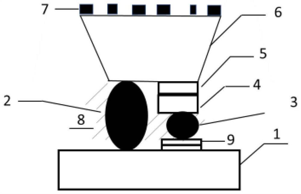
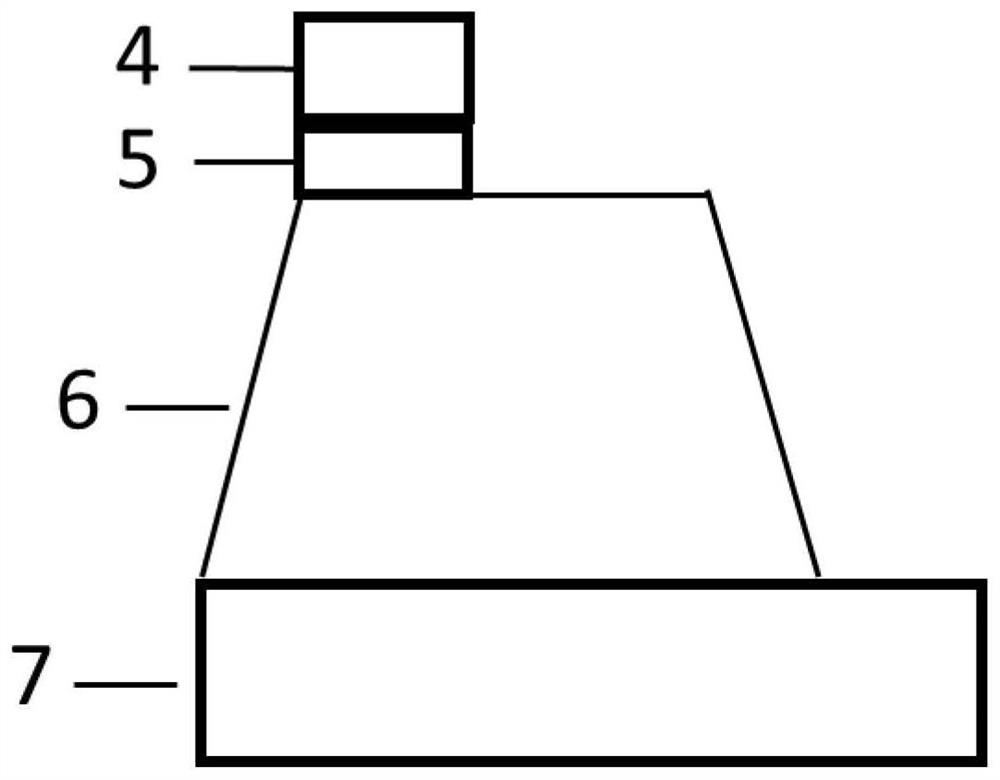
[0031] A surface-shaped flip-chip Micro LED provided in this embodiment includes a substrate 1 and an LED chip; the LED chip includes a p-GaN layer 4, an MQW (quantum well) layer 5, and an n- GaN layer 6; the width of the p-GaN layer 4 is equal to that of the MQW layer 5 and smaller than the width of the n-GaN layer 6, and the thickness of the n-GaN layer 6 gradually increases from top to bottom, forming inclined side walls Step structure; the lower surface of the n-GaN layer 6 is provided with a designed micro-nano structure 7;

[0032] The LED chip is flip-chip welded on the substrate-1 through a micro-bump structure;

[0033] The micro-bump structure includes micro-bump one 2, micro-bump two 3 and filling material 8, and the filling material 8 is filled around the micro-bump one 2 and micro-bump two 3; the filling material 8 is SU8 glue , Silicone SU8 glue or silicone.

[0034] The n-GaN layer 6 is connected to the substrate one 1 through the micro bump one 2; the p-GaN4 ...

Embodiment 2

[0041] A method for preparing a flip chip Micro LED provided in this embodiment includes the following steps:

[0042] (1) A sapphire sheet with a diameter of 1 inch is selected as the substrate 2 7 with a thickness of about 400 μm. An n-GaN layer 6 with a thickness of 2 μm and an MQW (InGaN / GaN layer) with a thickness of 100 nm are sequentially grown on the sapphire by MOCVD method. Quantum well) layer 5 and p-GaN layer 4 with a thickness of 200nm to form GaN LED epitaxial materials, such as figure 2 shown. The LEDs in the present invention are GaN-based LEDs, such as AlInGaN and InGaN LEDs, for producing blue and green light.

[0043] (2) Spin-coat photoresist on the p-GaN layer 4, use photoresist as a mask, and adopt ICP etching to etch the LED chip, ICP power 500W, RF power 150W, Cl 2 / BCl 3 40 sccm and 5 sccm respectively, spin-coat AZ4620 type photoresist with a thickness of 6 μm, and etch for 650 s. The etching depth reaches the upper surface of the n-GaN layer 6 t...


PUM

PropertyMeasurementUnit
angleaaaaaaaaaa
thicknessaaaaaaaaaa
thicknessaaaaaaaaaa

Abstract

The invention provides a surface shaping flip-chip bonding Micro LED and a preparation method thereof. The surface shaping flip-chip bonding Micro LED comprises a first substrate and an LED epitaxialmaterial. The LED epitaxial material sequentially comprises a p-GaN layer, an MQW layer and an n-GaN layer from top to bottom. The width of the p-GaN layer is equal to that of the MQW layer and is smaller than that of the n-GaN layer. The thickness of the n-GaN layer gradually increases from top to bottom to form an inclined sidewall step structure. A micro-nano structure is arranged on the lowersurface of the n-GaN layer. The LED epitaxial material is connected to the first substrate in a flip-chip bonding manner through a micro bump structure. The preparation method comprises the followingsteps: preparing an LED epitaxial material; performing etching to form an inclined sidewall step structure; connecting the step structure to a first substrate by flip-chip bonding; stripping a secondsubstrate of the epitaxial material; and preparing a micro-nano structure, thus finishing the preparation of the Micro LED device. The obtained Micro LED device has high light extraction efficiency, high display brightness and good display performance.

Description

technical field [0001] The invention relates to the field of optoelectronic technology, in particular to a surface shaping flip-chip welding Micro LED and a preparation method thereof. Background technique [0002] The display industry is a leading industry in the information age, with an annual output value of more than 100 billion U.S. dollars. Light-emitting diodes (LEDs) have gradually become the mainstream in the field of display lighting due to their irreplaceable advantages of energy saving, high efficiency, durability, and mercury-free. Micro-LED is considered to be the most potential display technology after TFT-LCD and AMOLED technology due to its excellent characteristics such as ultra-high resolution, high brightness, ultra-power saving and fast response. In Micro-LED display, the size of pixel unit is reduced to improve display accuracy and resolution. LEDs are similar to Lambertian light sources, with a larger light output angle. Trace-Pro software simulates ...

Claims


Application Information

Patent Timeline
Patent Type & Authority Patents(China)
IPC IPC(8): H01L33/32H01L33/06H01L33/20H01L33/62H01L33/00
CPCH01L33/0075H01L33/06H01L33/20H01L33/32H01L33/62
Inventor 汪炼成龙林云万荣桥胡泽林高祥
Owner NUOSHI TECH (SUZHOU) CO LTD
Why Eureka
Try Eureka