Surface shaping flip-chip bonding Micro LED and preparation method thereof
A flip-chip soldering and solder joint technology, applied in electrical components, circuits, semiconductor devices, etc., can solve the problems of increasing process steps, reducing pixel size, etc., to achieve the effect of improving performance, improving device heat dissipation, and high display brightness
- Summary
- Abstract
- Description
- Claims
- Application Information
AI Technical Summary
Problems solved by technology
Method used
Image
Examples
Embodiment 1
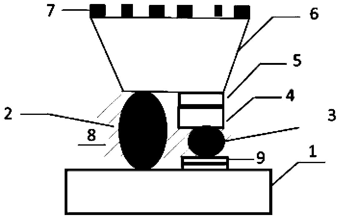
[0031] A surface-shaped flip-chip Micro LED provided in this embodiment includes a substrate 1 and an LED chip; the LED chip includes a p-GaN layer 4, an MQW (quantum well) layer 5, and an n- GaN layer 6; the width of the p-GaN layer 4 is equal to that of the MQW layer 5 and smaller than the width of the n-GaN layer 6, and the thickness of the n-GaN layer 6 gradually increases from top to bottom, forming inclined side walls Step structure; the lower surface of the n-GaN layer 6 is provided with a designed micro-nano structure 7;
[0032] The LED chip is flip-chip welded on the substrate-1 through a micro-bump structure;
[0033] The micro-bump structure includes micro-bump one 2, micro-bump two 3 and filling material 8, and the filling material 8 is filled around the micro-bump one 2 and micro-bump two 3; the filling material 8 is SU8 glue , Silicone SU8 glue or silicone.
[0034] The n-GaN layer 6 is connected to the substrate one 1 through the micro bump one 2; the p-GaN4 ...
Embodiment 2
[0041] A method for preparing a flip chip Micro LED provided in this embodiment includes the following steps:
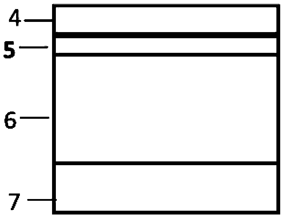
[0042] (1) A sapphire sheet with a diameter of 1 inch is selected as the substrate 2 7 with a thickness of about 400 μm. An n-GaN layer 6 with a thickness of 2 μm and an MQW (InGaN / GaN layer) with a thickness of 100 nm are sequentially grown on the sapphire by MOCVD method. Quantum well) layer 5 and p-GaN layer 4 with a thickness of 200nm to form GaN LED epitaxial materials, such as figure 2 shown. The LEDs in the present invention are GaN-based LEDs, such as AlInGaN and InGaN LEDs, for producing blue and green light.
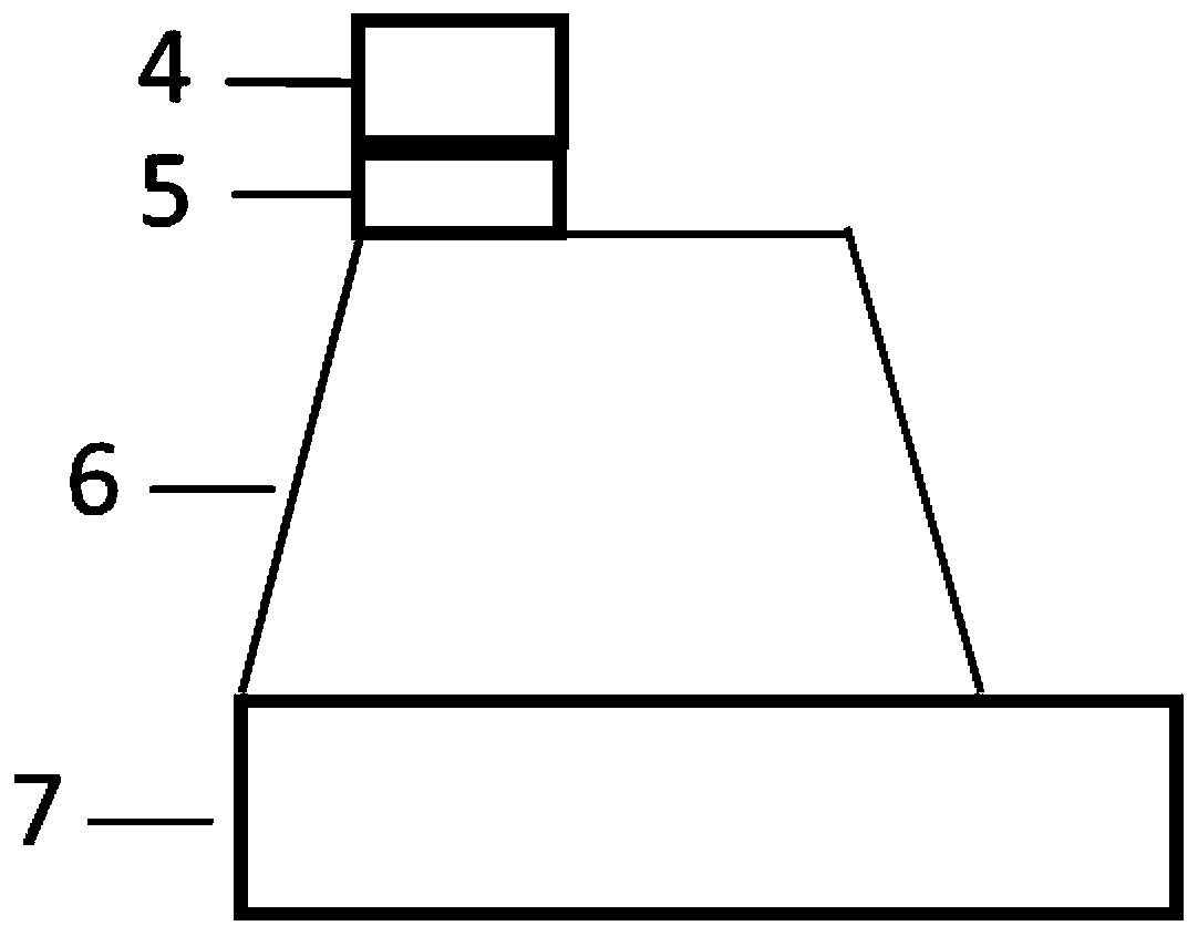
[0043] (2) Spin-coat photoresist on the p-GaN layer 4, use photoresist as a mask, and adopt ICP etching to etch the LED chip, ICP power 500W, RF power 150W, Cl 2 / BCl 3 40 sccm and 5 sccm respectively, spin-coat AZ4620 type photoresist with a thickness of 6 μm, and etch for 650 s. The etching depth reaches the upper surface of the n-GaN layer 6 t...
PUM
 Abstract
Description
Claims
Application Information


