

A mask assembly and a display device
A component and mask technology, applied in the direction of electrical components, electrical solid devices, semiconductor devices, etc., can solve problems that affect the display effect of the display area
- Summary
- Abstract
- Description
- Claims
- Application Information
AI Technical Summary
Problems solved by technology
Method used
Image

Examples
Embodiment 1
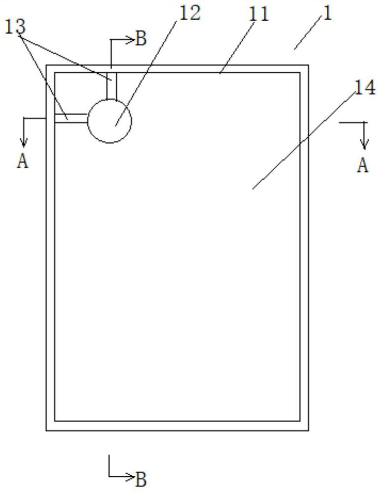
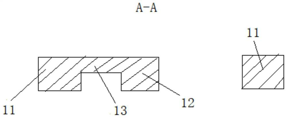
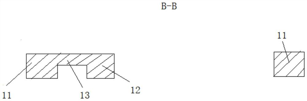
[0038] Such as figure 1 As shown, this embodiment describes a mask assembly, specifically a mask plate 1 for evaporation, which includes a mask frame 11, several island shielding parts 12 and bridges 13, the island shielding part 12 is connected to the mask frame 11 or the adjacent island shielding portion 12 through the bridge 13 . The mask frame 11 is supported on the peripheral surface of the substrate, that is, the mask frame 11 is not used for shielding the evaporation material, and an opening area 14 is formed in the mask frame 11 to allow the material to enter and deposit, and the island shielding portion 12 is arranged in the opening. The area 14 is used to shield the evaporation material to form a shielding area; wherein the substrate refers to the substrate to be evaporated, and the mask frame 11 in this embodiment is a square support plate, and an opening area is formed in the square support plate 14 and the shielding area formed by the island shielding part 12 and...
Embodiment 2
[0045] See attached Figure 6-7 , this embodiment describes a display device, which includes a display area 3, at least one non-display area 4 and a transitional display area 5, wherein the display area 3 is arranged around the non-display area 4; the transitional display area 5 Adjacent to the non-display area 4 and the display area 3 respectively, wherein the transition display area 5 connects the edges of the non-display area 4 and the display area 3 . When more than one non-display area 4 is provided, the transitional display area 5 can also connect two adjacent non-display areas 4 .
[0046] In this embodiment, the thickness of the first electrode of the transition display area 5 is less than or equal to the thickness of the first electrode of the display area 3, and the first electrode of the display area 3 and the first electrode of the transition display area 5 The electrodes are connected to form surface electrodes.
[0047] Wherein the display area 3 and the transi...
PUM
 Abstract
Description
Claims
Application Information