Thin film packaging structure and display panel

A thin-film packaging and display panel technology, which is applied to identification devices, semiconductor/solid-state device components, instruments, etc., can solve problems such as film layer separation, inorganic layer fracture, and large stress, so as to improve bending performance and service life. Ensure the stability of the package and increase the effect of stability

Active Publication Date: 2022-02-25
BOE TECH GRP CO LTD +1
View PDF10 Cites 0 Cited by
  • Summary
  • Abstract
  • Description
  • Claims
  • Application Information

AI Technical Summary

Problems solved by technology

[0003] At present, in order to isolate water and oxygen from entering OLED devices, thin film encapsulation (Thin Film Encapsulation) technology is often used to encapsulate them. The traditional thin film encapsulation structure includes inorganic layers and organic layers stacked in sequence. Therefore, the inorganic layer is prone to breakage or the film layer separation between the packaging film structures is easy to occur, which reduces the bendability of the display panel.

Method used


Image

  • Thin film packaging structure and display panel
  • Thin film packaging structure and display panel
  • Thin film packaging structure and display panel

Examples


Embodiment 1

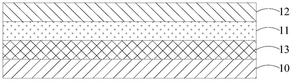
[0044] If the first inorganic encapsulation layer 10 of the thin film encapsulation structure is more likely to break or be separated from other film layers during the actual bending process of the display panel, then if figure 1As shown, the first inorganic adjustment layer 13 can be formed between the first inorganic encapsulation layer 10 and the organic encapsulation layer 11, so that the stress neutral layer at the bend can be shifted toward the first inorganic encapsulation layer 10, namely : The distance between the first inorganic encapsulation layer 10 and the stress-neutral layer is reduced, so that compared with the traditional scheme in which the first inorganic encapsulation layer 10 is directly combined with the organic encapsulation layer 11, under the same bending radius, The deformation of the first inorganic encapsulation layer 10 can be reduced, thereby alleviating the situation that the first inorganic encapsulation layer 10 is broken or separated from othe...

Embodiment 2

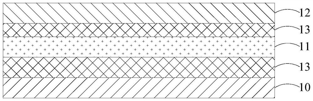
[0048] When the first inorganic adjustment layer 13 is silicon oxide and the second inorganic encapsulation layer 12 is silicon nitride, since the oxygen content of the first inorganic adjustment layer 13 is greater than the oxygen content of the second inorganic encapsulation layer 12, therefore, the first The contact angle between the inorganic adjustment layer 13 and the organic encapsulation layer 11 is smaller than the contact angle between the second inorganic encapsulation layer 12 and the organic encapsulation layer 11, and the bonding strength between the first inorganic adjustment layer 13 and the organic encapsulation layer 11 after curing can be Greater than the bonding strength between the second inorganic encapsulation layer 12 and the organic encapsulation layer 11 .

[0049] Based on this, if figure 2 As shown, compared with the first embodiment, in this embodiment, in addition to forming the first inorganic adjustment layer 13 between the first inorganic enca...

Embodiment 3

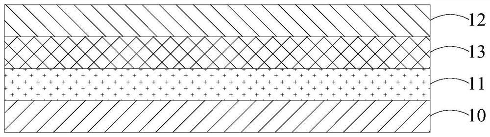
[0053] If the second inorganic encapsulation layer 12 of the thin film encapsulation structure is more likely to break or be separated from other film layers during the actual bending process of the display panel, the first inorganic adjustment layer 13 can be formed between the second inorganic encapsulation layer 12 and the other film layers. between organic encapsulation layers 11, such as image 3 shown; or the first inorganic adjustment layer 13 is formed on the side of the second inorganic encapsulation layer 12 away from the organic encapsulation layer 11, as Figure 4 or a first inorganic adjustment layer 13 is formed between the second inorganic encapsulation layer 12 and the organic encapsulation layer 11, and another first inorganic adjustment layer 13 is formed on the second inorganic encapsulation layer 12 away from the organic encapsulation layer 11 side, such as Figure 5 shown. Adopting these schemes can make the stress-neutral layer at the bend shift toward ...


PUM

PropertyMeasurementUnit
thicknessaaaaaaaaaa

Abstract

The present application relates to the field of display technology, in particular, to a thin film packaging structure and a display panel. The thin film encapsulation structure includes: a first inorganic encapsulation layer, used to cover the device to be encapsulated; an organic encapsulation layer, formed on one side of the first inorganic encapsulation layer; a second inorganic encapsulation layer, formed on a side of the organic encapsulation layer away from One side of the first inorganic encapsulation layer; at least one first inorganic adjustment layer, formed on the side of the first inorganic encapsulation layer away from the device to be encapsulated; wherein, the elasticity of the first inorganic adjustment layer The modulus is higher than the elastic modulus of the first inorganic encapsulation layer and the second inorganic encapsulation layer. This solution can increase the stability of the thin-film packaging structure during the bending process, so as to avoid the breakage of the thin-film packaging structure or the separation of the film layers, and ensure the packaging stability of the thin-film packaging structure, thereby improving the bending of the display panel performance and service life.

Description

technical field [0001] The present application relates to the field of display technology, in particular, to a thin film packaging structure and a display panel. Background technique [0002] As the application fields of flexible OLED (Organic Light-Emitting Diode, Organic Light-Emitting Diode, Organic Light-Emitting Diode, Organic Light-Emitting Diode) display panels continue to expand, the requirements for the reliability of flexible OLED devices in harsh environments are also getting higher and higher. [0003] At present, in order to isolate water and oxygen from entering OLED devices, thin film encapsulation (Thin Film Encapsulation) technology is often used to encapsulate them. The traditional thin film encapsulation structure includes inorganic layers and organic layers stacked in sequence. Therefore, the inorganic layer is prone to breakage or the film layer separation between the packaging film structures is easy to occur, which reduces the bendability of the displa...

Claims


Application Information

Patent Timeline
Patent Type & Authority Patents(China)
IPC IPC(8): H01L51/52H01L27/32
CPCH10K59/10H10K50/844H10K50/8445H10K50/858Y02E10/549H10K2102/351H10K77/111G02F1/133305G09F9/301H10K50/80H01L23/564H01L33/44H01L33/12G06F1/1641G06F1/1652H10K2102/00H10K2102/311
Inventor 蒋志亮王世龙文平
Owner BOE TECH GRP CO LTD
Why Eureka
Try Eureka