
Contactless online testing device for input impedance at each position of printed circuit board

An Input Impedance, On-Line Test Technology

Active Publication Date: 2019-12-03
BEIHANG UNIV
View PDF8 Cites 3 Cited by
  • Summary
  • Abstract
  • Description
  • Claims
  • Application Information

AI Technical Summary

Problems solved by technology

However, for the components, chips and circuit modules at each position of the printed circuit board, due to the limitation of the space size on the circuit board, if methods such as adding auxiliary circuits around the tested object or placing current calipers are used, the printed circuit will be damaged. The working state of the board itself is affected, and it cannot meet the broadband test requirements of input impedance

Method used


Image

  • Contactless online testing device for input impedance at each position of printed circuit board
  • Contactless online testing device for input impedance at each position of printed circuit board
  • Contactless online testing device for input impedance at each position of printed circuit board

Examples


Embodiment Construction

[0042] The following will clearly and completely describe the technical solutions in the embodiments of the present application with reference to the accompanying drawings in the embodiments of the present application. Obviously, the described embodiments are only for illustration, and are not intended to limit the present application.

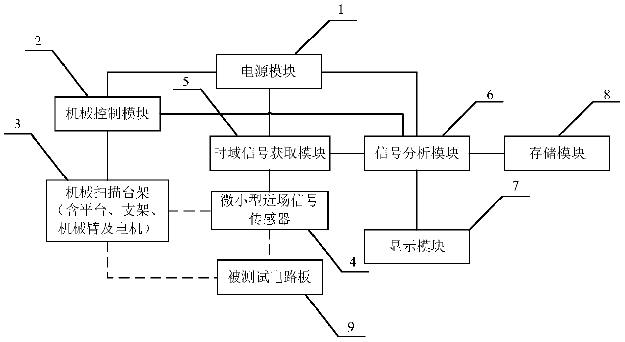
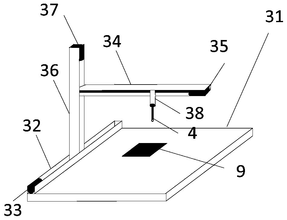
[0043] An embodiment of the present invention provides a non-contact on-line test device for input impedance at each position of a printed circuit board, such as figure 1 As shown, it includes: power supply module 1, mechanical control module 2, mechanical scanning platform (including platform, mechanical arm, motor and bracket) 3, miniature near-field signal sensor 4, time-domain signal acquisition module 5, and signal analysis module 6 , a display module 7 and a storage module 8; wherein, the solid line in the figure represents an electrical connection, and the dotted line represents a non-electric contact type physical contact, specifically:...


PUM


Abstract

The invention discloses a contactless online testing device for an input impedance at each position of a printed circuit board. The device comprises a mechanical scanning holder, a mechanical controlmodule, a microminiature near field signal sensor, a signal obtaining module, a signal analysis module, a display module, a storage module and a power module. Through utilization of the microminiaturenear field signal sensor and the signal obtaining module, near field magnetic field signals around input or output signal lines of a chip, a component and a circuit module at each position of a tested printed circuit board are coupled and obtained. Through utilization of the signal analysis module, the signals are processed, and the input impedances of the chip, the component and the circuit module at each position of the tested printed circuit board are solved, and corresponding amplitude frequency and phase frequency information is output. According to the device, through adoption of the contactless microminiature near field signal sensor, influence on a working state of the printed circuit board is low. The device is applicable to online testing of the input impedances of the chip, thecomponent and the circuit module at each position of the printed circuit board.

Description

technical field [0001] The invention relates to the technical field of electromagnetic signal characteristics, in particular to a device for testing the input impedance of components, chips and circuit modules. Background technique [0002] The analysis and control of electromagnetic emission at the board level is crucial to solve the electromagnetic compatibility of equipment level and system level. For printed circuit boards, the impedance mismatch at each position is an important reason for exceeding the external electromagnetic emission. In order to effectively control the external electromagnetic emission of the printed circuit board, it is necessary to analyze and design the input impedance at each position. However, the input impedance of each position of the printed circuit board is a hidden parameter of the printed circuit board, and it is related to the working state of the printed circuit board, so it is difficult to obtain it when working online. Therefore, onli...

Claims


Application Information

Patent Timeline
Patent Type & Authority Applications(China)
IPC IPC(8): G01R27/02
CPCG01R27/02
Inventor 苏东林徐辉
Owner BEIHANG UNIV
Learn More