Pixel circuit, driving method and display device

A technology of pixel circuits and driving transistors, applied in static indicators, instruments, etc., can solve the problems of uneven luminous brightness of display devices, high data voltage accuracy requirements, etc.

Active Publication Date: 2019-12-10
FUZHOU BOE OPTOELECTRONICS TECH CO LTD +1
View PDF7 Cites 8 Cited by
  • Summary
  • Abstract
  • Description
  • Claims
  • Application Information

AI Technical Summary

Problems solved by technology

[0003] Embodiments of the present invention provide a pixel circuit, a driving method, and a display device, which are used to improve the problem of uneven luminance in the display device, and improve the problem of high precision requirements for the data voltage output by the driving circuit

Method used


Image

  • Pixel circuit, driving method and display device
  • Pixel circuit, driving method and display device
  • Pixel circuit, driving method and display device

Examples


Embodiment 1

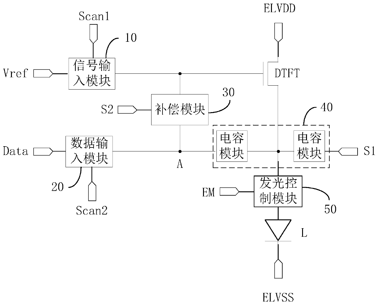
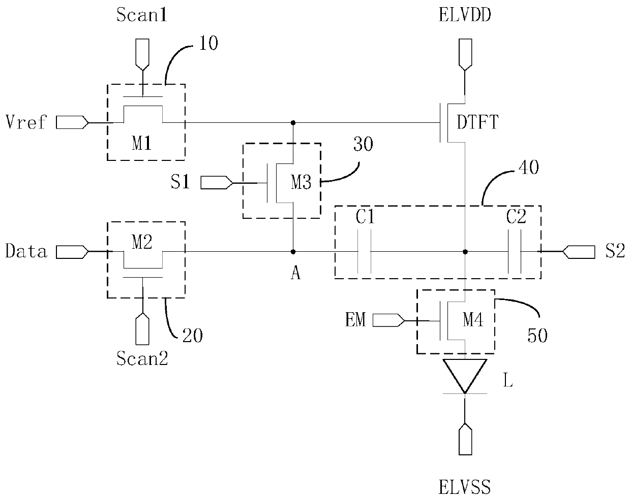
[0071] Below to image 3 The pixel circuit shown as an example, combined with Figure 5 The timing diagram of the circuit signals shown describes the working process of the above-mentioned pixel circuit provided by the embodiment of the present invention. Specifically, choose the Figure 5 There are three stages in the input timing diagram shown: the data input stage t1, the compensation stage t2, and the light emitting stage t3. Let the potential of the second electrode of the driving transistor DTFT be Vs.

[0072] In the data input phase t1, Scan1=1, Scan2=1, S1=0, EM=0, S2=1.

[0073] Because Scan1=1, the first switch transistor M1 is turned on; because Scan2=1, the second switch transistor M2 is turned on; because S1=0, the third switch transistor M3 is turned off; because EM=0, the fourth switch transistor M4 is turned off; Since S2=1, the voltage of S2 is VGH at this time, and the voltage of the second terminal of the second capacitor C2 is VGH.

[0074]Therefore, ...

Embodiment 2

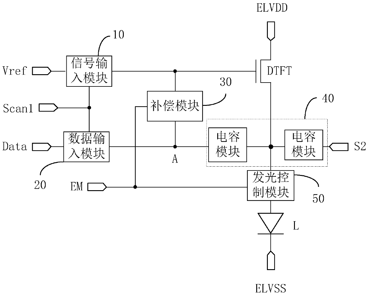
[0092] Below to Figure 4 The pixel circuit shown as an example, combined with Figure 6 The timing diagram of the circuit signals shown describes the working process of the above-mentioned pixel circuit provided by the embodiment of the present invention. Specifically, choose the Figure 6 There are three stages in the shown circuit signal timing diagram, the data input stage t1, the compensation stage t2, and the light emitting stage t3.

[0093] In the data input phase t1, Scan1=1, S1=0, S2=1.

[0094] The working process of this stage may be basically the same as the working process of the t1 stage in Embodiment 1, and will not be repeated here.

[0095] In the compensation phase t2, Scan1=0, S1=0, S2=0.

[0096] The working process of this stage may be basically the same as the working process of the t2 stage in Embodiment 1, and will not be repeated here.

[0097] In the lighting phase t3, Scan1=0, S1=1, S2=0.

[0098] The working process of this stage can be basic...


PUM


Abstract

The invention discloses a pixel circuit, a driving method and a display device. The pixel circuit comprises a signal input module, a data input module, a light-emitting control module, a compensationmodule, a capacitor module, a driving transistor and a light-emitting device. Through the mutual cooperation of the modules and the elements, the threshold voltage of the driving transistor can be compensated, so that the driving current for driving the light-emitting device L to emit light is not influenced by the threshold voltage of the driving transistor, and the problem of non-uniform light-emitting brightness caused by non-uniform threshold voltage is solved. Moreover, the voltage of the first power supply end can be compensated, so that the driving current is not influenced by the voltage of the first power supply end, and the problem of uneven light-emitting brightness caused by IR Drop of the first power supply end can be solved. Moreover, the range of the data voltage can be enlarged, and the voltage precision requirement of the driving circuit for generating the data voltage is reduced, so that the display effect is greatly improved.

Description

technical field [0001] The invention relates to the field of display technology, in particular to a pixel circuit, a driving method and a display device. Background technique [0002] The organic light emitting diode (Organic Light Emitting Diode, OLED) panel has the characteristics of bendability, high contrast ratio, low power consumption, etc., and has received extensive attention. Among them, the pixel circuit is the core technical content of the OLED panel, which has important research significance. Generally, the OLED in the OLED panel is driven to emit light by the current generated by the driving transistor in the pixel circuit. However, due to the limitation of the process and the increase of the service time, the threshold voltage Vth of the driving transistor will drift to different degrees, so that the OLED panel will have the problem of uneven luminance of the OLED. Moreover, due to the existence of IRDrop (voltage drop) in the OLED panel, the OLED panel will ...

Claims


Application Information

Patent Timeline
Patent Type & Authority Applications(China)
IPC IPC(8): G09G3/3208G09G3/3266G09G3/3291
CPCG09G3/3208G09G3/3266G09G3/3291G09G2320/0233G09G3/3233G09G2300/0819G09G2300/0852G09G2300/0861G09G2310/0251G09G2300/0426
Inventor 翁祖伟黄宇鹏许炜泽吴汉
Owner FUZHOU BOE OPTOELECTRONICS TECH CO LTD
Why Eureka
Try Eureka