A multiple quantum well structure, optoelectronic device epitaxial wafer and optoelectronic device

A multi-quantum well structure and optoelectronic device technology, applied in electrical components, semiconductor devices, circuits, etc., can solve the problems of low photon recombination efficiency, low internal quantum efficiency luminous rate, low electro-optical conversion efficiency, and low electro-optical conversion efficiency of light-emitting diodes. Achieve the effect of improving internal quantum efficiency, improving light recombination efficiency, and enhancing localization effect

Active Publication Date: 2021-12-14
UNIV OF SCI & TECH OF CHINA
View PDF5 Cites 0 Cited by
  • Summary
  • Abstract
  • Description
  • Claims
  • Application Information

AI Technical Summary

Problems solved by technology

[0003] Existing AlGaN-based UVLEDs often use a multi-quantum well structure with uniform composition and flat structure as the active region of the device (ie, the light-emitting region or the electron-hole recombination region), and the photon recombination efficiency of carriers in the two-dimensional quantum well structure Low, resulting in low internal quantum efficiency, external quantum efficiency and luminous efficiency of the device, and low electro-optical conversion efficiency of light-emitting diodes
Similar to light-emitting diodes, other optoelectronic devices such as light-emitting lasers and light-emitting detectors have problems with low internal quantum efficiency, external quantum efficiency, luminous efficiency, and low electro-optic conversion efficiency.

Method used


Image

  • A multiple quantum well structure, optoelectronic device epitaxial wafer and optoelectronic device
  • A multiple quantum well structure, optoelectronic device epitaxial wafer and optoelectronic device
  • A multiple quantum well structure, optoelectronic device epitaxial wafer and optoelectronic device

Examples


Embodiment Construction

[0026] In order to make the purpose, technical solutions and advantages of the present disclosure clearer, the present disclosure will be further described in detail below in conjunction with specific embodiments and with reference to the accompanying drawings.

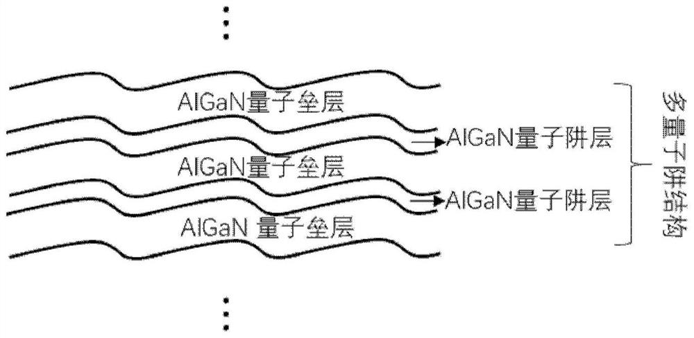
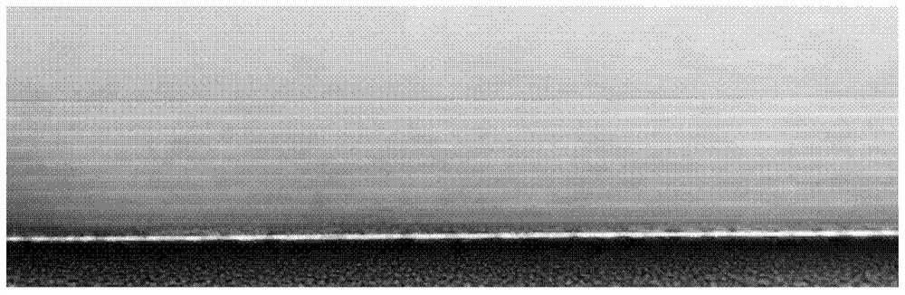
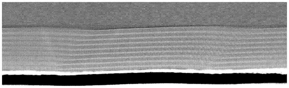
[0027] figure 1 A schematic diagram of the structure of the multi-quantum well structure provided by the embodiment of the present disclosure is schematically shown. refer to figure 1 , combined with Figure 2A and 2B , to describe the multi-quantum well structure of the present disclosure in detail.

[0028] The multi-quantum well structure is composed of alternately grown quantum well layers and quantum barrier layers, and each quantum well layer and quantum barrier layer is an uneven structure. The uneven structure is, for example, a wavy structure with the same thickness, or other structures with different thicknesses, or an asymmetric triangular wavy line structure.

[0029] Preferably, the included angle be...


PUM


Abstract

A multi-quantum well structure, a photoelectric device epitaxial wafer and a photoelectric device, wherein the multi-quantum well structure is composed of alternately grown quantum well layers and quantum barrier layers, and each quantum well layer and quantum barrier layer is an uneven structure. By setting the quantum well layer and quantum barrier layer of the multi-quantum well structure as a structure with uneven composition and uneven structure, the photorecombination efficiency, internal quantum efficiency, and luminous efficiency of carriers are improved, and it is applied to optoelectronics In device epitaxial wafers and optoelectronic devices, the preparation of high-power light-emitting diodes, high-power light-emitting lasers, and high-power light-emitting detectors has been realized.

Description

technical field [0001] The disclosure relates to the technical field of semiconductors, in particular to a multi-quantum well structure, an optoelectronic device epitaxial wafer and a photoelectric device. Background technique [0002] Ultraviolet Light Emitting Diode (UVLED) is mostly made of third-generation semiconductor materials. InAlGaN or BAlGaN materials have the characteristics of wide band gap and direct band gap. InAlGaN Or BAlGaN-based UVLEDs have broad application prospects in the fields of sterilization, disinfection, medical treatment and non-line-of-sight optical communication. AlGaN-based UV LEDs can achieve continuously adjustable emission wavelengths in the range of 200nm-360nm, and can be mass-produced on cheap silicon, sapphire, gallium nitride, aluminum nitride and silicon carbide substrates by heteroepitaxial methods. [0003] Existing AlGaN-based UVLEDs often use a multi-quantum well structure with uniform composition and flat structure as the active...

Claims


Application Information

Patent Timeline
Patent Type & Authority Patents(China)
IPC IPC(8): H01L33/06H01L33/24H01L33/32
CPCH01L33/06H01L33/325H01L33/24
Inventor 孙海定龙世兵刘明
Owner UNIV OF SCI & TECH OF CHINA
Why Eureka
Try Eureka