Array substrate and display panel
A technology of array substrate and bending area, which is applied in the direction of organic semiconductor devices, instruments, electrical components, etc., can solve problems such as abnormal picture, cracks, and increased stress concentration of source and drain layers, and achieve reduced risk of fracture and resistance to bending effect on ability
- Summary
- Abstract
- Description
- Claims
- Application Information
AI Technical Summary
Problems solved by technology
Method used
Image

Examples
Embodiment 1
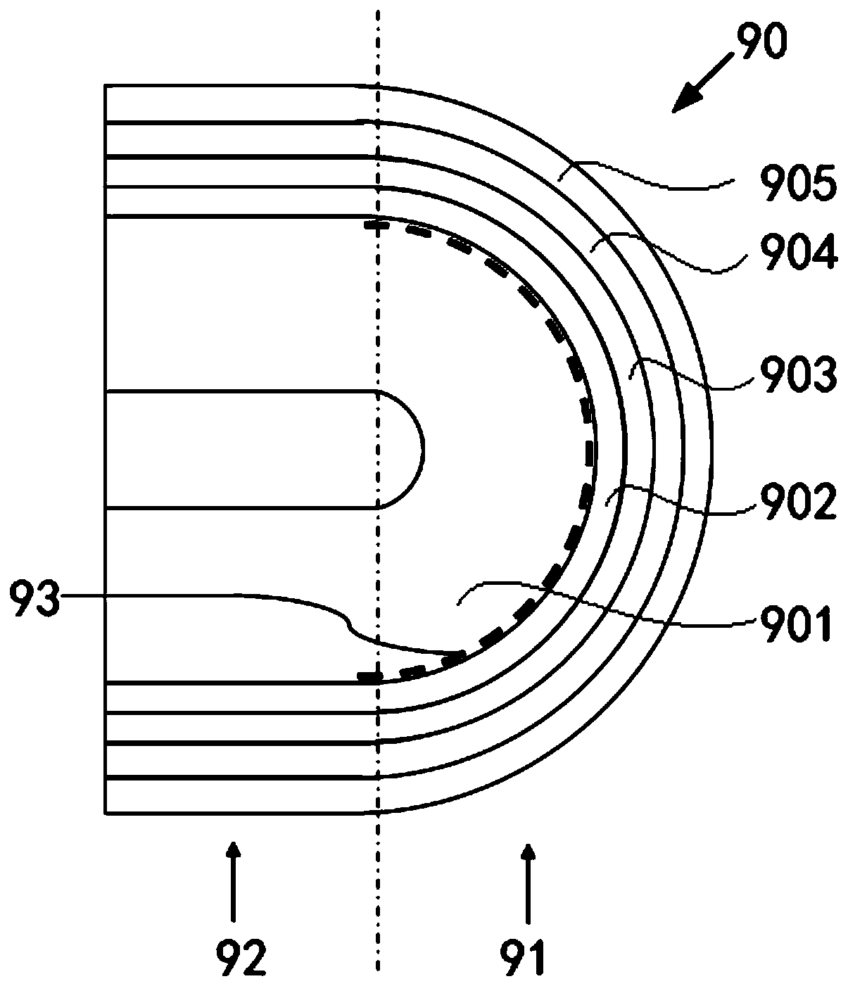
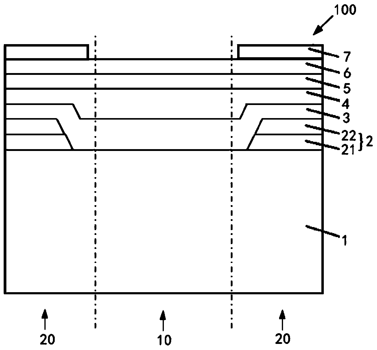
[0044] see figure 2 , image 3 As shown, the first embodiment of the present invention provides an array substrate 100 , which defines a bending area 10 and a non-bending area 20 . The non-bending region 20 includes a stacked flexible substrate layer 1, a composite buffer layer 2, a source-drain layer 3, a planar layer 4, and a pixel definition layer 5; specifically, as figure 2 As shown, the composite buffer layer 2 is located on the flexible substrate layer 1; the source and drain layer 3 is located on the composite buffer layer 2; the planar layer 4 is located on the source and drain layer 3; The pixel definition layer 5 is located on the planar layer 4 . Wherein the bending region 10 includes a flexible substrate layer 1, a source and drain layer 3, a flat layer 4 and a pixel definition layer 5 stacked; specifically, the source and drain layer 3 is located on the flexible substrate layer 1 ; The planar layer 4 is located on the source-drain layer 3 ; the pixel definit...
Embodiment 2
[0053] see Figure 4 , Figure 5 As shown, the second embodiment of the present invention provides an array substrate 100, including all the technical features of the first embodiment of the present invention, the difference is that the array substrate 100 of the second embodiment is set in the bending area 10 There is the composite buffer layer 2 , while the array substrate 100 of the first embodiment does not have the composite buffer layer 2 in the bending region 10 . Wherein, the thickness of the composite buffer layer 2 in the bending area 10 of the array substrate 100 of the second embodiment is smaller than the thickness of the composite buffer layer 2 in the non-bending area 20 .
[0054] The thickness of the composite buffer layer 2 in the bending region 10 of the array substrate 100 proposed by the second embodiment is reduced, but compared with the prior art, the source and drain layers 3 can still move down as a whole, away from the stress The closer the balance ...
Embodiment 3
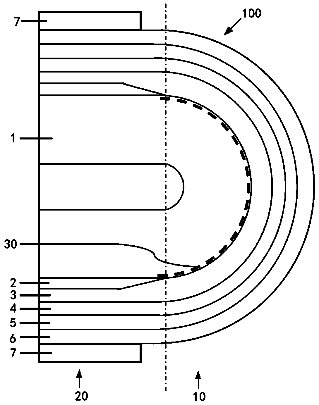
[0056] see Figure 6 As shown, in the third embodiment of the present invention, an array substrate 100 is provided, which includes all the technical features in the first embodiment of the present invention, the difference is that an organic layer 8 is provided in the third embodiment, and the organic layer 8 Formed in the non-bending region 20 and adjacent to the bending region 10, a part of the organic layer 8 covers the composite buffer layer 2 and another part is formed on the flexible substrate layer 1, and the source and drain layers 3 covering the organic layer 8. In other words, the organic layer 8 is formed at the junction of the composite buffer layer 2 and the bending region 10 . The organic layer 8 can be used as a transition to buffer the bending region 10 and the non-bending region 20 to prevent circuit breakage caused by excessive stress at the etching edge of the composite buffer layer 2 .
[0057] In this embodiment, the material of the organic layer 8 incl...
PUM
 Abstract
Description
Claims
Application Information
 - R&D Engineer
- R&D Manager
- IP Professional
- Industry Leading Data Capabilities
- Powerful AI technology
- Patent DNA Extraction
Browse by: Latest US Patents, China's latest patents, Technical Efficacy Thesaurus, Application Domain, Technology Topic.
© 2024 PatSnap. All rights reserved.Legal|Privacy policy|Modern Slavery Act Transparency Statement|Sitemap