Preparation method of through hole structure and preparation method of three-dimensional memory

A memory and three-dimensional technology, which is applied in the fields of electrical solid-state devices, semiconductor devices, semiconductor/solid-state device manufacturing, etc., can solve problems affecting device reliability, SEG damage, and damage to epitaxial growth layers, etc.

Inactive Publication Date: 2020-01-17
YANGTZE MEMORY TECH CO LTD
View PDF6 Cites 2 Cited by
  • Summary
  • Abstract
  • Description
  • Claims
  • Application Information

AI Technical Summary

Problems solved by technology

However, in practical applications, due to process reasons, there are often seams in the filling of the sacrificial material in the lower via hole; in the process of etching the upper via hole and removing the sacrificial material in the lower via hole, due to the Existence, the etching reaction will damage the epitaxial growth layer (Selective Epitaxial Growth, SEG) at the bottom of the via hole, causing SEG damage, which will seriously affect the reliability of the device

Method used


Image

  • Preparation method of through hole structure and preparation method of three-dimensional memory
  • Preparation method of through hole structure and preparation method of three-dimensional memory
  • Preparation method of through hole structure and preparation method of three-dimensional memory

Examples


preparation example Construction

[0045] Based on this, an embodiment of the present invention provides a method for preparing a through-hole structure; for details, please refer to image 3 . As shown, the method includes the following steps:

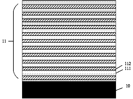
[0046] Step 201, providing a base structure, the base structure including a first stacked layer;

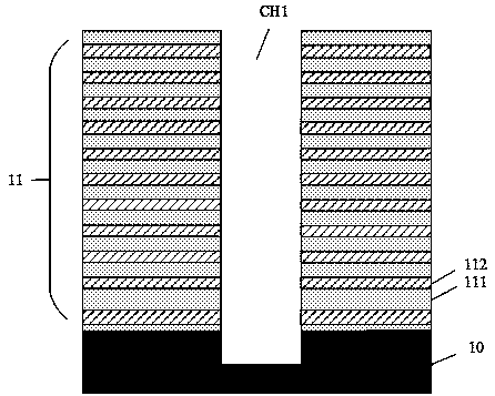
[0047] Step 202, etching the first stacked layer to form a first through hole;

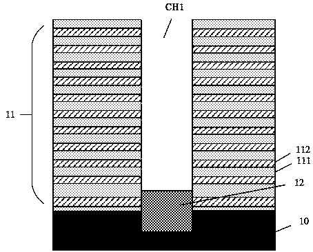
[0048] Step 203, forming an epitaxial growth layer at the bottom of the first through hole;

[0049] Step 204, forming an etching barrier layer in the first through hole, the etching barrier layer covering at least the surface of the epitaxial growth layer;

[0050] Step 205, forming a filling structure in the first through hole;

[0051] Step 206, forming a second stack layer on the first stack layer;

[0052] Step 207, etching the second stacked layer to form a second through hole communicating with the first through hole;

[0053] Step 208, etching to remove the filling structure in ...


PUM

PropertyMeasurementUnit
thicknessaaaaaaaaaa

Abstract

The embodiment of the invention provides a preparation method of a through hole structure. The preparation method comprises the following steps: providing a substrate structure comprising a first stacking layer; etching the first stacking layer to form a first through hole; forming an epitaxial growth layer at the bottom of the first through hole; forming an etching barrier layer in the first through hole, wherein the etching barrier layer at least covers the surface of the epitaxial growth layer; forming a filling structure in the first through hole; forming a second stacking layer on the first stacking layer; etching the second stacking layer to form a second through hole communicated with the first through hole; etching to remove the filling structure in the first through hole; whereinthe etching selection ratio between the material of the etching barrier layer and any one of the following materials meets the etching barrier requirements: the second stacking layer, the filling structure and the oxide layer of the filling structure. In addition, the embodiment of the invention further provides a preparation method of the three-dimensional memory, and the preparation method comprises the steps in the preparation method of the through hole structure.

Description

technical field [0001] The invention relates to the technical field of semiconductors, in particular to a method for preparing a through-hole structure and a method for preparing a three-dimensional memory. Background technique [0002] With the development of technology, the structure of semiconductor devices is constantly updated and changed, and the traditional through-hole structure and its formation process are gradually unable to meet the functional requirements of new devices. For example, for three-dimensional memory devices, especially 3D NAND memory, as people's demand for high storage density increases, the number of stacked layers of devices is increasing; the channel hole (Channel Hole, CH) of three-dimensional memory devices It is usually necessary to etch the stack until the substrate structure is exposed; in this case, the increased number of stacked layers creates higher requirements and challenges for the etching process of CH. In order to deal with this p...

Claims


Application Information

Patent Timeline
Patent Type & Authority Applications(China)
IPC IPC(8): H01L21/311H01L27/115
CPCH01L21/31105H10B69/00
Inventor 霍宗亮姚兰杨号号高晶周文斌
Owner YANGTZE MEMORY TECH CO LTD
Why Eureka
Try Eureka