Ti-ga-sb phase change material, phase change memory and preparation method of ti-ga-sb phase change material

A phase change memory, ti-ga-sb technology, applied in the direction of electrical components, etc., can solve the problems affecting the application reliability and service life of phase change memory, crystallization temperature and low temperature of ten-year data retention, crystalline state and amorphous state Problems such as large density differences, to achieve ultra-fast phase transitions, improve volume stability, and reduce density differences

Active Publication Date: 2021-02-23
HUAZHONG UNIV OF SCI & TECH
View PDF9 Cites 0 Cited by
  • Summary
  • Abstract
  • Description
  • Claims
  • Application Information

AI Technical Summary

Problems solved by technology

However, the crystallization temperature and ten-year data retention temperature of existing phase change materials are relatively low. For example, the crystallization temperature of Ge-Sb-Te phase change material is 150°C, and the ten-year data retention temperature is 85°C. Poor thermal stability; this greatly restricts the application of phase change materials in extreme environments
[0004] At the same time, when the phase change memory material in the existing phase change memory is used, there is often a large density difference between the crystalline state and the amorphous state, for example, in the amorphous Ge-Sb-Te phase change material, The lone pair electrons of the chalcogenide Te element will lead to the formation of a large number of vacancies, which will cause a large number of voids in the phase change material, resulting in a large density difference between the crystalline state and the amorphous state, usually above 8%.
Such a large difference in phase change density has far exceeded the influence of thermal expansion and contraction of phase change materials, which can easily lead to voids in phase change materials during the phase change process, and these voids usually gradually gather at the electrodes during the working process. Detach the phase change material from the electrode, eventually causing device failure and affecting the application reliability and service life of the phase change memory

Method used


Image

  • Ti-ga-sb phase change material, phase change memory and preparation method of ti-ga-sb phase change material
  • Ti-ga-sb phase change material, phase change memory and preparation method of ti-ga-sb phase change material
  • Ti-ga-sb phase change material, phase change memory and preparation method of ti-ga-sb phase change material

Examples


Embodiment 1

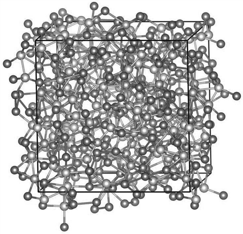
[0040] In this embodiment, the general chemical formula of the nano-Ti-Ga-Sb phase-change film material used in the phase-change memory is Ti x Ga y Sb 100-x-y , where x=9.7, y=18.5, that is, the chemical formula of Ti-Ga-Sb phase change material is Ti 9.7 Ga 18.5 Sb 71.8 .

[0041] The Ti-Ga-Sb nano film material in this embodiment is preferably prepared by magnetron co-sputtering.

[0042] Specifically, it is prepared by selecting the corresponding Ga-Sb alloy target and Ti elemental target for double-target co-sputtering. The Ga-Sb alloy target selected in this example is Ga 20 Sb 80 alloy target.

[0043] During preparation, high-purity inert gas is used as the sputtering gas, the volume percentage of high-purity inert gas reaches more than 99.999%, and the sputtering pressure is preferably adjusted to 0.5Pa; Pure argon was used as the sputtering gas. At the same time, Ga 20 Sb 80 The alloy target preferably adopts a DC power supply, and the power supply is 36W;...

Embodiment 2

[0064] In this embodiment, the preparation method of the Ti-Ga-Sb phase-change thin film material is the same as the above steps, the biggest difference is that the Ga in step S21 20 Sb 80 Alloy target replaced by Ga 30 Sb 70 Alloy target, and adjust the power of DC sputtering power supply for the Ti simple substance target in step S23 to 9W.

[0065] After the above magnetron co-sputtering process, Ti-Ga-Sb phase-change thin film materials with different thicknesses can be obtained according to the sputtering time. After quantitative analysis by X-ray photoelectron spectrometer (XPS), it can be known that the chemical composition formula of the film material obtained in the present embodiment is Ti 19.1 Ga 24.2 Sb 56.7 .

Embodiment 3

[0067] In this embodiment, the preparation method of the Ti-Ga-Sb phase-change thin film material is the same as the steps in the second embodiment, the difference is that the Ga in the step S21 30 Sb 70 Alloy target replaced by Ga 40 Sb 60 , the DC sputtering power supply of the Ti single target is still 9W.

[0068] After the above magnetron co-sputtering process, Ti-Ga-Sb phase-change thin film materials with different thicknesses can be obtained according to the sputtering time. After quantitative analysis by X-ray photoelectron spectrometer (XPS), it can be known that the chemical composition formula of the film material obtained in the present embodiment is Ti 19.1 Ga 30.6 Sb 50.3 .


PUM

PropertyMeasurementUnit
thicknessaaaaaaaaaa
thicknessaaaaaaaaaa
electrical resistanceaaaaaaaaaa

Abstract

The invention discloses a Ti-Ga-Sb phase-change material, a phase-change memory and a preparation method of the Ti-Ga-Sb phase-change material, belonging to the field of phase-change storage materials, and the Ti-Ga-Sb phase-change material is Ti, Sb , the chemical formula of Ga element composition is Ti x Ga y Sb 100‑x‑y The material is obtained by using Sb as the base material and doping Ti and Ga into the base material; wherein, x and y are the percentages of atoms, and 0<x<50, 0<y<50, 0 <x+y<60. The Ti-Ga-Sb phase-change material of the present invention has a simple and convenient preparation method, and compared with traditional phase-change materials, the prepared Ti-Ga-Sb phase-change material has a smaller difference in phase-change density, and can While ensuring the thermal stability of phase change materials, the crystallization efficiency of phase change materials is greatly improved, the stability and accuracy of information data storage of phase change materials are guaranteed, the efficiency of information storage of phase change memory is improved, and the service life of phase change memory is extended. At the same time, the functionality of the phase change memory is greatly improved.

Description

technical field [0001] The invention belongs to the field of phase-change memory materials, and in particular relates to a Ti-Ga-Sb phase-change material and a preparation method thereof, as well as the application of the Ti-Ga-Sb phase-change material in phase-change memory. Background technique [0002] In the era of big data, the status of memory is becoming more and more prominent. Both the storage of information data and the transmission of information data pose new challenges to traditional memory. The research and development of new memory has also become an important part of technological innovation. Phase change memory is an excellent non-volatile memory device, which has the characteristics of fast read and write speed, large capacity and low production cost. It is currently one of the most promising next-generation memory devices. Phase change memory mainly uses the resistance difference between the crystalline state and the amorphous state of the phase change mat...

Claims


Application Information

Patent Timeline
Patent Type & Authority Patents(China)
IPC IPC(8): H01L45/00
CPCH10N70/881H10N70/026
Inventor 徐明徐萌缪向水
Owner HUAZHONG UNIV OF SCI & TECH
Why Eureka
Try Eureka