Wafer curvature adjustment device and method

A technology for adjusting device and curvature, which is applied in the manufacture of electrical components, circuits, semiconductors/solid-state devices, etc. It can solve the problems that the direction of adjustment cannot be selected, and the adjustment of wafer curvature cannot be accurate, etc., to achieve adjustment and achieve curvature Effect

Active Publication Date: 2022-07-29
YANGTZE MEMORY TECH CO LTD
View PDF21 Cites 0 Cited by
  • Summary
  • Abstract
  • Description
  • Claims
  • Application Information

AI Technical Summary

Problems solved by technology

However, in the related art, the adjustment of the curvature of the wafer can only be adjusted in units of the plane where the wafer surface is located.
The direction of adjustment cannot be selected, that is, the adjustment of the wafer bow cannot be accurate to a specific direction on the plane of the wafer surface

Method used


Image

  • Wafer curvature adjustment device and method
  • Wafer curvature adjustment device and method
  • Wafer curvature adjustment device and method

Examples


Embodiment Construction

[0029] To make the objectives, technical solutions and advantages of the embodiments of the present invention clearer, the specific technical solutions of the invention will be described in further detail below with reference to the accompanying drawings in the embodiments of the present invention. The following examples are intended to illustrate the present invention, but not to limit the scope of the present invention.

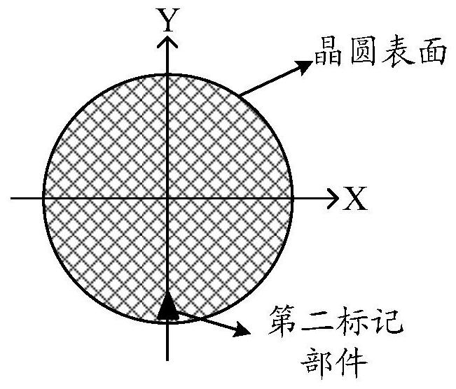
[0030] like figure 1 As shown, the X direction mentioned in the embodiment of the present invention refers to the X-axis direction of the plane where the wafer surface is located; the Y direction mentioned in the embodiment of the present invention refers to the Y-axis direction of the plane where the wafer surface is located.

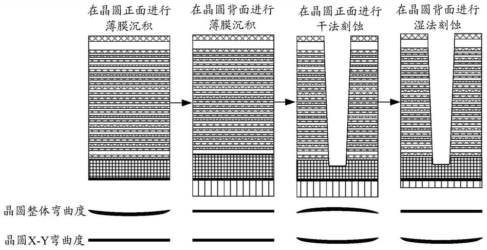
[0031] In the related art, the curvature of the wafer can be obtained by measuring the curvature of the wafer. Generally, the curvature of the wafer is characterized by the curvature of at least two aspects of the wafer, that is, th...


PUM


Abstract

Embodiments of the present invention provide an apparatus and method for adjusting the curvature of a wafer. When etching the thin film deposited on the wafer disposed on the fixed body of the circular curvature adjusting device, the thin film deposited on the wafer is adjusted by heating the heating part of the wafer curvature adjusting device in the first The etching thickness in the direction is used to adjust the curvature of the wafer in the first direction; the heating component is arranged on the fixed body. In this way, the curvature of the wafer in a specific direction can be adjusted.

Description

technical field [0001] The present invention relates to the technical field of semiconductors, and in particular, to a device and method for adjusting the curvature of a wafer. Background technique [0002] In the manufacturing process of semiconductors, it is necessary to carry out a multi-layer thin film deposition process on the front side of the wafer and to perform an etching process on the deposited multi-layer thin film. These processes will cause the wafer to warp, and the wafer warpage (expressed as bow in English) will lead to a series of adverse consequences. Therefore, controlling the wafer curvature within a reasonable range has huge economic benefits and research value. [0003] In the related art, the stress of the wafer is generally improved by depositing a specific film (such as a silicon nitride film, a silicon oxide film, etc.) on the back of the wafer and etching the deposited film to adjust the curvature of the wafer. . However, in the related art, th...

Claims


Application Information

Patent Timeline
Patent Type & Authority Patents(China)
IPC IPC(8): H01L21/67H01L21/311
CPCH01L21/67063H01L21/67103H01L21/31111
Inventor 白靖宇
Owner YANGTZE MEMORY TECH CO LTD
Why Eureka
Try Eureka