Electromagnetic shielding film, circuit board, and method for preparing electromagnetic shielding film

An electromagnetic shielding film and printed circuit board technology, applied in the electronic field, can solve problems such as grounding failure, inability to interfere with charge derivation, and inability to realize shielding function, so as to achieve the effect of realizing shielding function and ensuring normal derivation

Pending Publication Date: 2020-02-07
GUANGZHOU FANGBANG ELECTRONICS
View PDF0 Cites 0 Cited by
  • Summary
  • Abstract
  • Description
  • Claims
  • Application Information

AI Technical Summary

Problems solved by technology

However, at high temperature, due to the expansion of the conductive adhesive layer, the conductive particles in the conductive adhesive layer that were originally in contact with each other or the conductive particles that were originally in contact with the circuit board ground layer were pulled apart, resulting in grounding failure, and the interference charge could not be quickly exported. , the shielding function cannot be realized

Method used


Image

  • Electromagnetic shielding film, circuit board, and method for preparing electromagnetic shielding film
  • Electromagnetic shielding film, circuit board, and method for preparing electromagnetic shielding film
  • Electromagnetic shielding film, circuit board, and method for preparing electromagnetic shielding film

Examples


Embodiment Construction

[0036] The technical solutions in the embodiments of the present invention will be clearly and completely described below in conjunction with the accompanying drawings in the embodiments of the present invention. Apparently, the described embodiments are only some of the embodiments of the present invention, not all of them. Based on the embodiments of the present invention, all other embodiments obtained by persons of ordinary skill in the art without making creative efforts all belong to the protection scope of the present invention.

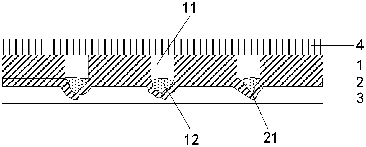
[0037] see figure 1 , is a structural schematic diagram of an angle of the electromagnetic shielding film provided in Embodiment 1 of the present invention;

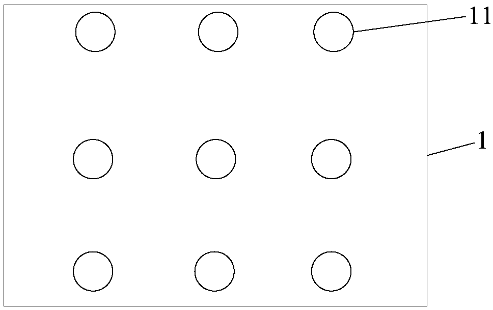
[0038] see figure 2 , is a structural schematic diagram of another angle of the electromagnetic shielding film provided by Embodiment 1 of the present invention;

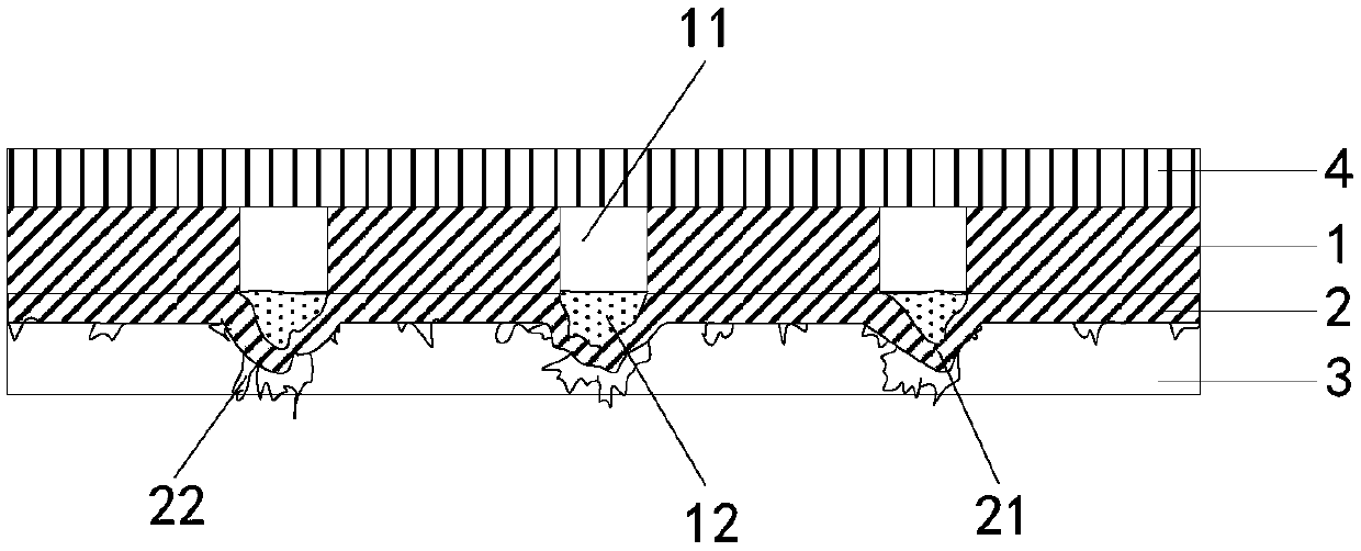
[0039] combine figure 1 and figure 2 As shown, the electromagnetic shielding film includes a resin film layer 1, a fir...


PUM

PropertyMeasurementUnit
heightaaaaaaaaaa
thicknessaaaaaaaaaa
thicknessaaaaaaaaaa

Abstract

Embodiments of the invention provide an electromagnetic shielding film, a circuit board and a method for preparing the electromagnetic shielding film, and the electromagnetic shielding film is characterized by comprising a resin film layer, a first shielding layer and an adhesive film layer, wherein the resin film layer is provided with a first through hole, a resin protrusion is disposed at the first through hole, and the resin protrusion is formed by the solidification of the resin flowing from one side to the other side of the first through hole; the first shielding layer is disposed on theside of the resin film layer adjacent to the resin protrusion and covers the resin protrusion, so as to form a convex portion on the position of the outer surface of the first shielding layer corresponding to the resin protrusion; the adhesive film layer is provided on the side of the first shielding layer away from the resin film layer, and the convex portion extends into the adhesive film layer, so that the convex portion can ensure that the first shielding layer can pierce the adhesive film layer smoothly and contact the ground of the circuit board during the pressing process, thereby ensuring that the interference charges are normally derived and the shielding function is realized.

Description

technical field [0001] The invention relates to the field of electronics, in particular to an electromagnetic shielding film, a circuit board and a method for preparing the electromagnetic shielding film. Background technique [0002] With the rapid development of the electronics industry, electronic products are further developed toward miniaturization, light weight, and high-density assembly, which greatly promotes the development of flexible circuit boards, thereby realizing the integration of component devices and wire connections. Flexible circuit boards can be widely used in industries such as mobile phones, liquid crystal displays, communications and aerospace. [0003] Driven by the international market, functional flexible circuit boards dominate the flexible circuit board market, and an important indicator for evaluating the performance of functional flexible circuit boards is electromagnetic shielding (Electromagnetic Interference Shielding, referred to as EMI Shi...

Claims


Application Information

Patent Timeline
Patent Type & Authority Applications(China)
IPC IPC(8): H05K1/02H05K9/00
CPCH05K1/0216H05K9/0022H05K9/0084
Inventor 苏陟
Owner GUANGZHOU FANGBANG ELECTRONICS
Why Eureka
Try Eureka